Because of the Thanksgiving holiday in the U.S., TI E2E™ design support forum responses may be delayed from November 25 through December 2. Thank you for your patience.

This thread has been locked.

If you have a related question, please click the "Ask a related question" button in the top right corner. The newly created question will be automatically linked to this question.

CD4046B: CD4046B VCO calculation problem

Part Number: CD4046B

Hi, I got the input from customer about VCO calculate even I check to application guide. But still confused about it. Can you help double check on it?

Thanks


Application -  4046 Phase Locked Loop as an FM Demodulator (Using phase comparator I  for VCO with OFFSET)

To distinguish the input range in 400KHz,

Case 1: If input(pin14) range locate in Ftyp to Fmax, the P1(pin2) =1,

Case 2: If input (pin 14) range locate in Ftyp to Fmin, the P1(pin2)=0

Q1: How to calculate the value of R1,R2 and C1 to get the correct frequency as below?

Fmin=310KHz

Ftyp=383.8KHz

Fmax=471.194KHz

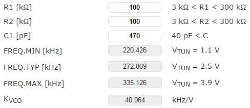
There have another tool we calculated as below. Is it correct?

Q2: If we do not need external low pass filter, can we keep floating? Currently, we connect R3,C2 as below.

R3 =18K,C2=220P ,fc=40.1KHz


 Application - 4046 Phase Locked Loop for clock generator(Using phase comparator I  for VCO with OFFSET)

Use CD4046B pin2 to generate the frequency about 300KHz, MCU GPIO will send the signal to CD4046B pin5 (Inhibit) and pin14 keep external pull high.

In case pin5 (Inhibit) receive =1 high from MCU, P1 should output the frequency.

Q3 : In this case, can we floating the Pin2 and pin9 if do not connect to low pass filter?

        R1,R2,C1 show as below.


  • The picture cannot show on my post, so I can send it to mailbox if you need it.
  • Hi Jimmy,

    The best way to post images on here is to go the the 'rich formatting' option at the bottom right, then click the "Insert/Edit Media" button on the toolbar. I have found that copying/pasting an image in doesn't work well.

  • Hello Jimmy,

    How are you coming to calculate the values shown?
    In order to select the R1, R2, and C1, you need to refer to Figure 9 in the application note to get the correct values.
    R1 you used to select the center frequency, while R2 you used to select the offset. C1 is something to help define the center and offset frequencies for the corresponding R1 and C1.

    Is there a reason you don't want to have an R3 and C2 value? Are you not using feedback to the VCO and just setting the VCO biasing based on the R2 value?
    The feedback to the VCO should be a DC signal or else you will get a lot of switching which will affect the bias point of the VCO as shown in Figure 8 of the application note.

    If you are doing FM demodulation, then you need to set the R1, R2, and C1 for the center carrier frequency, and the R3 and C2 are selected for the capture frequency based on the equation in the app note for Fc on page 18.

    Best,
    Michael