This thread has been locked.

If you have a related question, please click the "Ask a related question" button in the top right corner. The newly created question will be automatically linked to this question.

CD4046B: CD4046B:

Part Number: CD4046B
Other Parts Discussed in Thread: SN74LV4046A

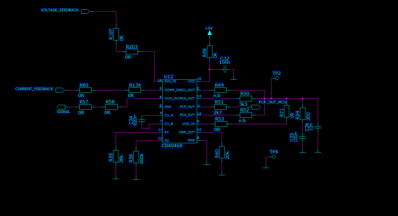
The resistors values used to set the Fmax and Fmin does not produce the same frequency band for different ICs.Is there an way to get the frequency band from fmay to fmin with always the same frequecies with different ICs. My fmin= 35.4kHz and fmax is = 36,6kHz , a bang of 1,2kHz.I am using 680kOhms and 36kOhms resistors with C = 820pF.

  • Hi Tahir,
    Do you mean that the CD4046B has a different frequency band with the same resistor, or that you are using multiple different devices (for example, SN74HC4046, SN74LV4046A, etc.) and they have different frequency bands?

    What are the new frequencies / how much of a difference do you see?
  • Hello


    I have two boards with CD4046B both produce different values of fmin and fmax with same resistor values. Fmin on one board is 35kHz and on the other board is 35.3kHz (300Hz difference). Fmax on one board is 36.71 kHz and on the other board is 36.3(410 Hz difference).

    For practical purpose this is a very big difference at least for my application.

  • Hi Tahir,
    It's not uncommon to see differences of that scale (~0.1%) with a part like this. If you need more accuracy, I would recommend using a different method for frequency generation. These parts (integrated logic PLLs) were designed/built a long time ago and won't be the best solution for a modern/accurate communication system -- they are probably the lowest cost option though. There are always trade-offs for cost vs performance.
  • Can I apply voltage at these pins to adjust the range?
  • Hey Tahir,
    The resistor supplies a constant current to an internal current mirror - adding a voltage likely won't have the effect you desire.
  • Is it possible to use a current sink to control the current at pin 11 and 12 and then control fmin and fmax with current sink? This ways I can use microcontroller to control the Limits by applying different voltages to the current sink.Do you have any such current sink?

  • Hey Tahir,
    You are welcome to try this if you like -- you're going beyond the recommended operation, so I can't really help with that. There's nothing stopping you from experimenting though.

    The TI logic team doesn't make constant current sinks -- you would have to either design one with existing components (for example, a JFET) or find a company that does make them.

    It's unlikely that this will change the performance of the device though... every IC has slight variations due to process, and they will never have exactly the same output. This is part of designing system -- tolerances must always be included in the design. As I mentioned previously, if this device doesn't meet your tolerance requirements, you can look at better solutions out there.... some of TI's clocking solutions have incredible accuracy. My team doesn't deal with those though -- I only work with the older parts like the one we've been discussing.
  • I am applying a signal at the input of the ref pin 14( a voltage signal) and a signal at the comparator pin 3(a current signal) and I am watching the output at pin 13 of phase detector II.Phase dector has a RRC and C filter  I see that the phase detector output pin 13 starts gettting a DC Offset and then saturate to 5V. Why it saturates to 5V after giving correct pulses of Phase difference at the beginning? What can I do to avoid the Problem? I am usinf resitors at pin 11 and pin 12 to Limit the frequency in the range from 36400Hz to 36600Hz. 

  • Hi Tahir,
    Please provide a schematic of your circuit (include test connections if you can) and scope shots of the input and output waveforms that are giving you trouble.

    It's quite difficult to troubleshoot a circuit I can't see with signals described in text.
  • Hey Tahir,
    I haven't heard back from you in a while. I'm going to go ahead and close this thread. If you need additional assistance, you can respond directly to this thread -- or if it has been locked, you can use the "+ Ask a related question" button in the top right to continue the conversation.
  • I am sending you the diagram of the oscilloscope waveforms. When I apply Signal at the Ref(pin 14) and the comparator pins(pin 3) I get Signals on the PD1 (pin2) and PCP OUT (pin1) but I do not get any Signal on the PD2 PC2 OUT (Pin 13). I have changed many ICs but it does not work. 

    Yellow is Comparator, Blue SIG_IN (pin 14) and Red is PD1(Pin 2). 

    Yellow is Comparator, Blue SIG_IN (pin 14) and Red is PCP_OUT(Pin 1). 

    Yellow is Comparator, Blue SIG_IN (pin 14) and Red is PD II(Pin 13). 

  • Thanks for the detailed response - this is very helpful to me.

    PC2 can be problematic in some systems.  Here's the logical structure:

    I know the logic is a little hard to follow on this -- I cleaned up everything except PC2 here to try to help.  Note that the output can drive either HIGH, LOW, or not at all (Hi-Z). This is specifically controlled by the rising edges of the incoming signals.  The problem occurs when you get 2 or more rising edges on one signal while the other signal only has only 1 rising edge. This will cause the logic to get, for lack of a better term, out of cycle.  Usually, this is how the system would work:

    (1)  If SIG_IN rising edge leads COMP_IN rising edge, then the pFET at the output turns ON and the output is driven HIGH -- until the COMP_IN rising edge is seen and the output switches back to High-Impedance mode.

    (2) If COMP_IN rising edge leads SIG_IN rising edge, then the nFET at the output turns ON and the output is driven LOW -- until the SIG_IN rising edge is seen and the output switches back to High-Impedance mode.

    (3)  If the two signals are in phase, both signals clock at the same time and both DFF's get reset at the same time, keeping the output in the High-Impedance state. 

    As long as the inputs remain consistent, there's no issue. The output voltage will be increased when COMP_IN leads SIG_IN and decreased in the opposite case.

    A problem can occur if two edges come in on one input, in which case the phase difference will be read as the opposite of what it actually is. It's possible for the device to become "confused" and end up forcing the output the wrong direction, creating a positive feedback loop that just rails out the output.

    The best method I have seen to prevent this issue is to use the PC1 output instead, or to force the  device into the other mode of operation by putting multiple triggers on the opposite input to the one that is 'stuck.'

    I put together a state machine diagram to help explain. Hopefully it doesn't just add confusion.

    So, in this diagram, you can see that's it's possible to be in S1, then get a double trigger on SIG_IN and end up in S3 when you really _want_ to be in S2.  This will result in a reversal of the desired output (S2 to S3 oscillation instead of S1 to S2 oscillation), and the output gets 'stuck' at the rail.

  • I dont think it is the Problem which you are mentioning. I have connected a  pull up and a pull down resistors  on the PD2 output (Pin13). Now you can see that it is working but with an Offset of 2.5V which brings the VCO at the centre frequency and then a small negative pulse cannot bring it down to the Zero Phase. There is somthing wrong the IC circuit. There seems to be no flip flop state Problem. With pullp resistors I cannot make the Phase Zero but brings it slightly below the centre frequency. Is there any solution that the PD2 works without Pullup and pull down resitsors in standard way.

    Blue is Comparator, Yellow is Reference and the red is the PD2 Output after pull up and pull down with 2k resistors.

  • Hi Tahir,

    In my opinion, your latest scope shot and explanation continues to agree with my description of the issue.

    This scope shot shows that the device is driving the output LOW between (1) and (2), and the output is in high-impedance between (2) and (3), allowing the resistor divider to take over and hold the line at ~Vcc/2. This indicates that the device is operating in state S1 (from my earlier diagram) between (1) and (2), and S2 between (2) and (3).

    My assumption is that you need the PC2 output to drive HIGH (in S3) between 2 and 3 to fix the phase imbalance, but the device is stuck oscillating between S1 and S2, when it should be oscillating between S2 and S3 to fix the imbalance.

  • I cannot observe the difference in my diagram and the Figure 10 on the data sheet of CD4046B. The figure 10 is behaving exactly as my diagram so the states is right between 2 and 3 it cannot go high as in Figure 10 of data sheet.
  • Yes, the logic diagram in the datasheet shows exactly what you have in the scope shot -- ie the part is doing exactly what it's supposed to be doing under this circumstance.

    Perhaps I have misunderstood the issue?

    Here's a markup of the datasheet to match my state diagram:

    At (1) the SIG_IN rising edge switches PC2 into S1, switching on the pFET at the output. At (2) the rising edge at COMP_IN switches the device into S2, putting the output in Hi-Z mode. When both edges are seen at the same time (3), the device remains in S2. At (4) when the COMP_IN signal has a rising edge first, the device switches from S2 to S1, forcing the output low, and then it returns to S2 when SIG_IN goes high again.

    This is all the correct operation of the device, and matches what you're showing.

  • The state hi impedance means no voltage at the pin pd2 as both inner switches are off. This can be achieved only if i do not connect external pull up an pull down resistors. My question is that the part works as in the figure 10 and gives no voltage when high impedance only if i use it in a standard way when vco output is connected to reference input or comparator input. If I give external signals to the reference and comparator inputs then the pdase detector 2 give no voltage no matter what is the phase difference as shown in my earler diagrams. I only get three states high, low and middle point 2.5v when i use external pull up and pull down on pd2 pin with pure external inputs. In this case I get 2.5 v when high impedance is present. This brings problem as in high impedace no voltage should come. The problem is why the part does not work without external pull up and pull down when vco out is not used as one of the  phase detector 2 inputs.pd2 does not produce any voltage without external pull up and pull down if external signals are used on pd2. I have already sent you all diagrams. Pd2 works correctly without external pull up and pull down resistors if vco output is used as one of the pd2 inputs. I hope you now understand what i am trying to ask you in my last emails.        

  • "The state hi impedance means no voltage at the pin pd2 as both inner switches are off."
    "This brings problem as in high impedace no voltage should come."

    That is incorrect -- there will always be a voltage at the pin PC2. You are correct that the inner switches are off though. When a pin is placed in a high-impedance state it means that the pin will neither source nor sink current. This means that the CD4046B will not be changing the voltage at that pin, but that doesn't mean the voltage will disappear, nor does it mean that the voltage cannot change. Kirchhoff's laws still apply to the circuit.

    "If I give external signals to the reference and comparator inputs then the pdase detector 2 give no voltage no matter what is the phase difference as shown in my earler diagrams."

    Your earlier diagrams show that the PC2 output is driving LOW or Hi-Z and are not reaching the HIGH state. I have explained repeatedly and in detail why this occurs... and your own tests have shown that the device is operating properly (from the most recent scope shot).

    PC2 is a logical state machine, and you must treat it as such with the appropriate initialization or it will not work correctly.