This thread has been locked.

If you have a related question, please click the "Ask a related question" button in the top right corner. The newly created question will be automatically linked to this question.

CD4046B: frequency synthesizer using CD4046B

Part Number: CD4046B
Other Parts Discussed in Thread: CD40106B, CD4013B, CD4002B

Hello,

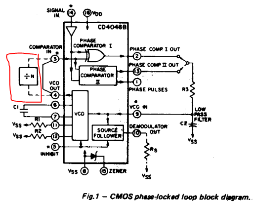
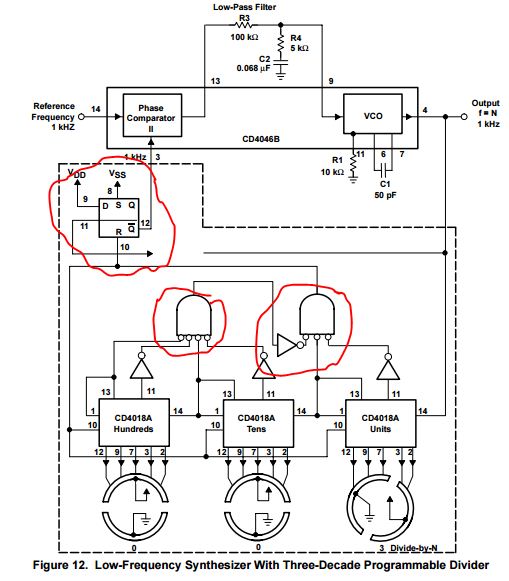
I wish to design frequency synthesizer using CD4046B. I referred the data sheet CD4046 where instruction about developing frequency synthesizer using CD4046 is give but some parts are unclear. I did not understand frome where to get those d and sr flipflop

  • Hello Pratik,

    Can you either post a screenshot showing what part is confusing to you, or give me a specific page number/quote from the text of the datasheet so I can find the confusing reference?

    My guess is that you are referring to the external clock division identified here:

    That division block refers to an external flip-flop or counter.

  •  Hello Emrys

    i have encircled the doubtful component which IC should i use for the flip flop and the AND gates please give me the reference of IC as i am pure beginner in feild of synthesizer. Any help would be highly appreciated

  • Hi Pratik,
    Pin 11 of the D-flip flop should be connected to the output of the VCO (pin 4 of the CD4046B).
    The D-flip flop is a CD4013B, and the logic can be created with a CD4002B (4-input NOR gate) and a CD40106B (hex inverter).

    I'm not sure why the logic diagram was drawn with NAND gates. You can replace the NANDs with NOR gates and it simplifies the circuit (since the inverted inputs are all eliminated). That drops the number of inverters required from 11 to 4. That means the circuit can be achieved with 7 chips (3x CD4018A, 1x CD4013B, 1x CD4002B, 1x CD40106B, 1x CD4046B)
  • Hello Emrys,

    Thank you so much for the reference of the IC's. It was of great help to proceed with the design.

    I was trying to simulate the design on proteus after the completion of the schematic when i try to run the schematic i do not get any waveform on the virtual oscilloscope available in proteus. by reference to google i came to know that to start the internal VCO i need to connect pin no.5 i.e INHIBIT pin to ground please correct me if I am wrong. After connecting the pin no % to ground i just get a square wave of 1 KHz on the output of VCO. Please help me in with the simulation of the design so that i can proceed with the actual implementation of the project.

    Also can i simulate this design on WEBENCH designer of TI.

  • Hi Pratik,
    The INHIBIT pin (pin 5) needs to be driven low to enable the VCO and the source follower (demodulator output, pin 10 - which needs to be terminated with a 10kohm resistor if unused). This information is on page 1 of the datasheet in the 'VCO' section.

    I'm not familiar with Proteus, so I'm not sure what model you are using for the CD4046B. I'm afraid that the CD4046B is a very old device which was not originally designed by TI (we acquired this device from Harris Semiconductor). Due to the age and process, we do not have a simulation model for it.
  • Hi Emrys,

     thank you so much for your reply and your valuable time i will get to you back after i get some good results. Thank you so much.

  • I look forward to seeing your results :)