This thread has been locked.
If you have a related question, please click the "Ask a related question" button in the top right corner. The newly created question will be automatically linked to this question.
Hello,
Maybe someone can shed a bit of light...
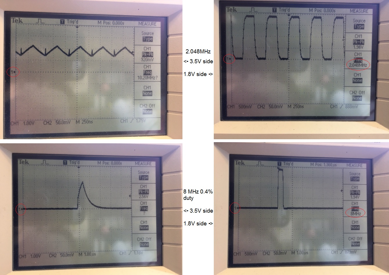
I have a TXB0108. VCCa (pin 2) is tied to 1.8V and VCCb (pin 19) is tied to 3.5V.
On pin 9 (A8), I have a 1.8V square 2.048MHz 50% duty signal coming-in and I expect to get the same frequency on pin 12 but with at 3.5V.
However, when I put my oscilloscope on pin 12, instead, instead of geting the nice 3.5V 2.048MHz signal, I get an approximate 1v pk-pk triangular wave with a DC offset of around 1.8V (so triangular waveform wings from around 1.3V to 2.2V).
Same idea with pin 8 where I input an 8kHz 5% (this time it's five, not fifty) duty signal... on the high side pin 13, this time, the low-to-high transition is a half triangle and the high-to-low side is a round slope (whole triangle sort of like the shape of a shark fin).
I really don't understand what can cause this behaviour. I tied OE pin to 1.8V and I used a 0.1uF cap on each supply.
What am I missing?
Thanks!
Benoit
Hi again,
Here's an update hoping it helps... I've done some more tests and I think I can rule-out the CODEC because I cut the physical trace on the PCB going from the TXB to the CODEC to make sure that the TXB outputs are isolated (physically disconnected) and I still have the garbled signals.
I've attached images from my oscilloscope screen.
FYI, in case it helps, my oscilloscope is a Tektronix TDS220 and my probes are Circuit Test OP-100A with the following specs (in case you wonder if my probes have an effect on the signal when I monitor it):
Input Resistance: x1 1M Ohm / x10 10M Ohm
Input Capacitance: x1 56pF / x10 13pF
Compensation Range: 10-30pF
Cable Length: 120cm
Operating Temperature: 0 to 50°C
The pictures from my oscilloscope screen for both signals for you to see.
Unfortunately I am not authorized to share the schematics but what I can say is that these two connections in particular are very straightforward.
The other I/O signals on that same TXB0108 work just fine but note that they are simple I/O lines getting toggled once in a while as opposed to the "problematic" ones being clock signals.
On either side of the TXB0108 on the PCM lines, there aren't any capacitors or resistors;
So to re-cap:
Modem out perfect 2.048MHz 50% duty (top-right image) > TXB0108 in 1.8V > TXB0108 out 3.5V > Lower-amplitude 2.048MHz triangular waveform with DC offset (top-left image)
Modem out perfect 8kHz 0.4% duty (bottom right image) > TXB0108 in 1.8V > TXB0108 out 3.5V > 8kHz 0.4% duty shark-fin waveform (bottom left image)
On this same circuit, I have a second TXB0108 with unused lines. So after cutting the trace to the modem signals, I soldered a mini piece if wire from the modem's PCM BCLK signal to the unused 1.8V input on the secondary TXB. Its output is not tied to anything. When I put my probe on the output, I get the exact same result. So I've ruled-out the original TXB0108 IC because the secondary behaves exactly the same.
Could it just be the oscilloscope probe corrupting the signal when I touch the line but when I remove it, the signal is fine but I just don't know? Am I beating a dead horse and I don't know it?
Any idea or suggestions?
Thanks again,
Benoit