This thread has been locked.

If you have a related question, please click the "Ask a related question" button in the top right corner. The newly created question will be automatically linked to this question.

TMS570LC4357: Optimization issue for F021

Part Number: TMS570LC4357
Other Parts Discussed in Thread: RM48L952

Hi,

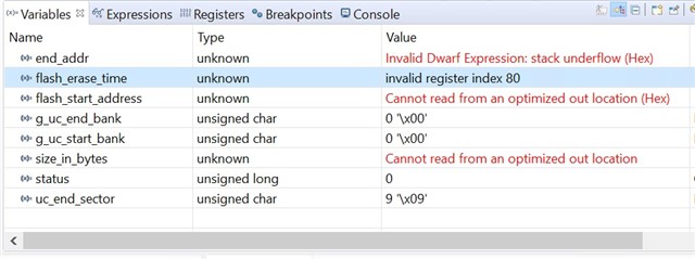
I am trying to erase and program data into the L2FMC Bank 0 and Bank 1 sectors using the library provided. With optimization level O0, seeing that both the operations are successful while using optimization levels O1 and O2, seeing that there is an exception. The operations were performed before enabling the instruction and data caches. Please provide me the solution of how to avoid the dependencies on the optimization level in performing operations on the internal flash. The VCLK used is 180MHz.

Thank you,

Tirumala.

  • Hi Tirumala,

    What error did you get when opt_level=1 or 2?

  • With optimization level O0, seeing that both the operations are successful while using optimization levels O1 and O2, seeing that there is an exception.

    Are the functions which which call the F021 API in RAM, as well the F021 API functions being placed in RAM?

    In CCS/RM46L852: jump to prefetchEntry when used Fapi_issueProgrammingCommand it was found that:

    1. The functions which call the F021 API functions also need to run from RAM, to avoid getting prefetch aborts.
    2. When the functions which call the F021 API were in flash, a prefetch abort occurred when attempted to step over the F021 API calls, but didn't cause an abort when single stepped the instructions of the F021 API. This suggests the cause of the prefetch abort is timing sensitive, which may explain why optimisation makes a difference.
  • Thank you Gillon for the response.

    Are the functions which which call the F021 API in RAM, as well the F021 API functions being placed in RAM?

    Earlier, I have tried the function(which calls F021 API functions) which was running from flash and F021 API functions were running from RAM.

    Based on your reply, I tried running the function (which calls F021 API functions) from RAM using optimization level O1.

    As I couldn't place the complete code here, I would like to provide the scenario in an instance. Kindly consider.

    Assume that the function A() has F021 API function calls, and B() calls A(). The sequence is B() --> A() --> F021 API functions. As per the reply

    In CCS/RM46L852: jump to prefetchEntry when used Fapi_issueProgrammingCommand it was found that:

    1. The functions which call the F021 API functions also need to run from RAM, to avoid getting prefetch aborts.
    2. When the functions which call the F021 API were in flash, a prefetch abort occurred when attempted to step over the F021 API calls, but didn't cause an abort when single stepped the instructions of the F021 API. This suggests the cause of the prefetch abort is timing sensitive, which may explain why optimisation makes a difference.

    I have tried running B() from flash and A() runs from RAM. When the control has to go from B() to A(), i.e. control has to shift from flash to RAM, the code is entering into an exception when tried to source code step-in or step-over or given a free run. Only the disassembly step-in is happening but even then, the variables are showing errors similar to variables in the screenshot below that "Cannot read from an optimized out location".

    Is this a kind of timing issue again?

    Please consider the additional try I have given for the same:

    As part of F021 erasing or programming, while loops exist to wait until the FMSTAT register to be zero. The timeouts for such loops are provided as per the datasheet based on the bank number. I am using the RTI module to capture those timeouts and the timeouts are provided as 10% more than what is provided in the datasheet as a tolerance. So trying with the approach in using timeout-related functions in the F021 source code, the exception is seen and there is no issue seen when the timeout-related functions are completely avoided but the timeouts are required in my application as this is the safety-critical system. Could you please suggest a solution how to avoid the exception in this case with the optimization level greater than 0 and including the timeouts?

    Thank you,

    Tirumala.

  • I have tried running B() from flash and A() runs from RAM. When the control has to go from B() to A(), i.e. control has to shift from flash to RAM, the code is entering into an exception when tried to source code step-in or step-over or given a free run.

    How is the code copied from flash to RAM?

    It sounds like an issue with either:

    1. How the code is copied from flash to RAM, resulting in incorrect instructions being executed in RAM.
    2. If execute permission has been given in the MMU settings for the RAM.

    See TMS570LC4357: Moving a function to RAM for things which can cause issues.

  • How is the code copied from flash to RAM?

    All the flash functionalities are copied and run from RAM using the linker file.

    .ram_code : AT (NEXT_LOAD_ADDR)
    {
    __RAM_CODE_START = .;
    *(.ram_code)
    KEEP (*f021_api.o(.text .text.*))
    KEEP (*fsm_enable_main_eeprom_sectors.o(.text .text.*))
    KEEP (*f021_erase.o(.text .text.*))
    KEEP (*f021_init_flash_banks.o(.text .text.*))
    KEEP (*f021_program.o(.text .text.*))
    KEEP (*f021_read.o(.text .text.*))
    KEEP (*f021_set_active_bank.o(.text .text.*))
    KEEP (*f021_utils.o(.text .text.*))
    } > RAM_CODE

    RAM_CODE origin is 0x08034D00 of length 0x00005BFF, 2kb which is sufficient to hold the functions.
    Also the code which calls the flash functions are run from RAM using __attribute__((noinline, section(".ram_code"))).

    Please make a note that the GCC compiler is used.

    If execute permission has been given in the MMU settings for the RAM.

    The execute permissions were given in the MMU.

    I have also tried to clean the cache as mentioned in  

    but found no improvement.

    Please suggest.

    Thank you,

    Tirumala.

  • All the flash functionalities are copied and run from RAM using the linker file.
    Please make a note that the GCC compiler is used.

    Can you confirm which version of the GCC compiler is being used?

    I wasn't aware that the GCC run-time start code contained functionality to copy such sections from FLASH to RAM at initialisation.

    Can you use the debugger to check if the code has actually been copied to RAM?

  • I wasn't aware that the GCC run-time start code contained functionality to copy such sections from FLASH to RAM at initialisation.

    Looking back at the example project RM48L952_GCC_FEE_read_write for a RM48L952, which copied the F021 API code from FLASH to SRAM, the sys_main.c had to copy the F021 code from FLASH to SRAM with the following:

    /* Symbols defined by linker script to copy flash API functions from the load address in flash to the run address in sram */
    extern char _sflashAPI;
    extern char _siflashAPI;
    extern char _eflashAPI;
    
    /* USER CODE END */
    
    /** @fn void main(void)
    *   @brief Application main function
    *   @note This function is empty by default.
    *
    *   This function is called after startup.
    *   The user can use this function to implement the application.
    */
    
    /* USER CODE BEGIN (2) */
    /* USER CODE END */
    
    void main(void)
    {
    /* USER CODE BEGIN (3) */
        unsigned int BlockNumber;
        unsigned int BlockOffset, Length;
        unsigned char *Read_Ptr=read_data;
    
        unsigned int loop;
    
        /* Copy flash API functions from flash to RAM */
        memcpy (&_sflashAPI, &_siflashAPI, &_eflashAPI - &_sflashAPI);

    And the sys_link.ld linker script had the following in the SECTIONS:

      .flashAPI :
      {
        . = ALIGN(4);
    
        _sflashAPI = .;         /* create a global symbol at data start */
        *Fapi_UserDefinedFunctions.o (.text*)
        *F021_API_CortexR4_LE_V3D16.lib:* (.text*)
    
        . = ALIGN(4);
        _eflashAPI = .;            /* define a global symbol at data end */
      } >RAM AT> FLASH_API

    Maybe the above example helps.

        /* used by the startup to initialize flashAPI */
       _siflashAPI = LOADADDR(.flashAPI);
    
      .flashAPI :
      {
        . = ALIGN(4);
    
        _sflashAPI = .;         /* create a global symbol at data start */
        *Fapi_UserDefinedFunctions.o (.text*)
        *F021_API_CortexR4_LE_V3D16.lib:* (.text*)
    
        . = ALIGN(4);
        _eflashAPI = .;            /* define a global symbol at data end */
      } >RAM AT> FLASH_API

  • Thanks for the response, Chester Gillon.

    The linker script mentioned is similar to what I had mentioned in my previous response, where all the object files related to F021 functionalities are copied to RAM. While debugging, I could see that the functions are running from the RAM locations.

  • Hi Chester Gillon, could you please let me know the probable solution for the optimization issue for F021 operations found, if any.

    Thank you in advance!

  • Hi Chester Gillon, could you please let me know the probable solution for the optimization issue for F021 operations found if any.

    Thank you in advance!

  • Hi Chester Gillon, could you please let me know the probable solution for the optimization issue for F021 operations found if any.

    I'm not sure on the cause of the optimization issue from the available information. Are you able to post an example program which shows the failure?

  • Hi Chester Gillon,

    As I cannot provide the complete code here, I am providing the sample code with the comments explaining the functionality performed. Only the flash erase and programming calls is provided. Kindly consider.

        #define CONST_3FF   __asm__ __volatile__("CONST_3FF  .word 0x3ff");
        #define CONST_7FFF  __asm__ __volatile__("CONST_7FFF .word 0x00007fff");
    
        #define CACHE_CLEAN __asm__ __volatile__(" MRC p15, #1, r0, c0, c0, #1 \n"  \
        " ANDS R3, R0, #0x07000000 \n"     \
        " MOV R3, R3, LSR #23 \n"          \
        " BEQ Finished \n"                 \
        " MOV R10, #0 \n"                  \
        "Loop1: \n"                        \
        " ADD R2, R10, R10, LSR #1 \n"     \
        " MOV R1, R0, LSR R2 \n"           \
        " AND R1, R1, #7 \n"               \
        " CMP R1, #2 \n"                   \
        " BLT Skip \n"                     \
        " MCR p15, #2, R10, c0, c0, #0 \n" \
        " ISB \n"                          \
        " MRC p15, #1, R1, c0, c0, #0 \n"  \
        " AND R2, R1, #7 \n"               \
        " ADD R2, R2, #4 \n"               \
        " LDR R4, = 0x3FF \n"           \
        " ANDS R4, R4, R1, LSR #3 \n"      \
        " CLZ R5, R4 \n"                   \
        " MOV R9, R4 \n"                   \
        "Loop2: \n"                        \
        " LDR R7, = 0x7FFF \n"           \
        " ANDS R7, R7, R1, LSR #13 \n"     \
        "Loop3: \n"                        \
        " ORR R11, R10, R9, LSL R5 \n"     \
        " ORR R11, R11, R7, LSL R2 \n"     \
        " MCR p15, #0, R11, c7, c10, #2 \n"\
        " SUBS R7, R7, #1 \n"              \
        " BGE Loop3 \n"                    \
        " SUBS R9, R9, #1 \n"              \
        " BGE Loop2 \n"                    \
        "Skip: \n"                         \
        " ADD R10, R10, #2 \n"             \
        " CMP R3, R10 \n"                  \
        " BGT Loop1 \n"                    \
        " DSB \n"                          \
        "Finished:")
    
     
    void cache_clean()
    {
    	CACHE_CLEAN;
    	return;
    }
    
    
    void entry_point()
    {
        // - pre-initializations for data, BSS sections and constuctors
    	// - Copy code from ROM to RAM, the code that should be executed from RAM
    
        // - Enable CPU bus event export
    
        // - reset handler for the types of reset
    
        // - Work around after checking if there were ESM group3 errors during power-up and clearing it
        //   These could occur during eFuse auto-load or during reads from flash OTP
        //   during power-up. Device operation is not reliable and not recommended
        //   in this case.
    
        // - setting up the PLL
    
        // - Release the peripherals from reset and enable clocks to all peripherals.
    
        // - PINMUX initialization and settings
    
        // - Initializing and Setting up the flash with HCLK 
    
        // - Trimming of LPO
    	
        // - Clock mapping
    
        // - Power on initialization of system clock
    
        // - Configure and setup the EMIF
    
        cache_clean();
    
        // - Pre- Initializations for data, BSS sections and constuctors
    
        // - Copy code from ROM to RAM, the code that should be executed from RAM
    
    
        flash_op();
    }
    
    
    uint32 flash_data[256 * 8];
    
    __attribute__((noinline, section(".ram_code"))) void flash_op(void)  // To run from the RAM location. Please find the attached code of linker file after the F021 API functions 
    {
        // - Initializing and Setting up the flash with HCLK 
    
        // - initialization of system clock
    
        // - Perform L2 SRAM single bit and multi bit ECC tests
    
        // - Perform flash single bit and multi bit ECC tests
    
        // - Install exception handlers in RAM location
    
        // - Initialize VIM
    
        // - Initialize ESM to configure system response to error conditions signaled to the ESM group1
    
        // - MPU initialization as below:
        //       Internal flash - Region 0 -  size 4MB - Outer and Inner write-through, no write-allocate non-shareable type and Privileged/User read-only mode.
        //       Internal SRAM  - Region 1 -  size 512KB - Outer and Inner write-through, no write-allocate non-shareable type and with full access mode.
        //       Internal Flash (Flash ECC, OTP and EEPROM accesses) - Region 2 - size 8MB - device, non-shareable type, writes in User mode generate permission faults access and never executes.
    	
    	// Note: The remaining MPU initializations are excluded here
    
        for(uint32 i = 0UL; i < (256UL * 8UL); i++)
        {
            flash_data[i]   = 0xAA552233UL;
            flash_data[i+1] = 0x33449988UL;
            flash_data[i+2] = 0xAA125623UL;
            flash_data[i+3] = 0x34459189UL;
            i += 3;
        }
    
        if(FapiBlockErase(0x60000, 8192UL) /* Erase the flash from 0x60000 of size 8MB.*/)
        {
            FapiBlockProgramEcc(0x60000, &flash_data, (4UL * 1024UL * 2UL));
        }
    
        // - Enable Instruction cache and data cache
        
        while(1);
    }

    And the flash API functions are as below:

    uint32 FapiBlockErase(uint32 FlashStartAddress, uint32 SizeInBytes)
    {
        // Compute the bank number based on the start address and the size provided. 
    
        // Initialize the F021 based on the start bank where the flash start address lies and the end bank where the end address (calculated based on the size) resides.
    	
    	// For each sector, perform erase operation. After performing erase operation of each sector, status of the FMSTAT register is collected if it becomes zero within the provided timeouts. If the time is exceeding the provided limit, then the further erase of sectors is not performed and the status of erase operation is not successful.
    	// Based on the computed bank number, the timeouts are provided as below:
        // Maximum erase time for main banks is 4.4 sec for sector erase as per the datasheet.
        // Maximum erase time for EEPROM is 8.8 sec for sector erase as per the datasheet.
         
    	// Return the status of the erase operation.
    }
    
    uint32 FapiBlockProgramEcc(uint32 FlashStartAddress, uint32 DataStartSddress, uint32 SizeInBytes)
    {
        // 1. Compute the bank number based on the start address and the size provided.  
    
        // 2. If the flash bank has been initialized in flash erase function, do not perform the initialization. Otherwise, initialize the flash based on the start bank where the flash start address lies and the end bank where the end address (calculated based on the size) resides.
    
        // 3. If the initialization is done, perform the programming byte by byte using the FlashStartAddress, DataStartSddress and SizeInBytes. After performing program operation on each byte, status of the FMSTAT register is collected if it becomes zero within the provided timeouts. If the time is exceeding the provided limit, then the further programming of sectors is not performed and the status of programming operation is not successful.
    	
    	// 3. Based on the computed bank number, the timeouts are provided as below:
        //    Maximum program time for 4MB internal flash main banks is 21.23 sec as per the datasheet.
        //    Maximum program time for 128KB EEPROM bank is 2.86 sec as per the datasheet.
    
    	//    Return the status of the program operation.
    }
    

    The above flash API functions and all the flash-related files/operations are copied to RAM and are executed from RAM. The linker script for the execution from RAM is as below:
    .ram_code : AT (NEXT_LOAD_ADDR)
    {
    __RAM_CODE_START = .;
    *(.ram_code)
    KEEP (*F021Api.o(.text .text.*))
    KEEP (*fsm_enable_main_eeprom_sectors.o(.text .text.*))
    KEEP (*f021_erase.o(.text .text.*))
    KEEP (*f021_init_flash_banks.o(.text .text.*))
    KEEP (*f021_program.o(.text .text.*))
    KEEP (*f021_read.o(.text .text.*))
    KEEP (*f021_set_active_bank.o(.text .text.*))
    KEEP (*f021_utils.o(.text .text.*))
    } > RAM_CODE
    __RAM_CODE_SIZE = (SIZEOF(.ram_code) / 4);

    The code is compiled using the GCC compiler version 4.2.3. The level of optimization can be chosen by the user. When level 0 is used, the erase/programming is done with the provided timeouts. No issues with it.

    When the level of optimization is increased (I tried with levels 1 and 2), then I am seeing the issues in those operations. So I had tried removing the usage of timeouts where I am able to get those operations done (with levels 1 and 2). As the system is safety-critical, timeouts are necessary to be implemented. The timeouts are used with the help of the RTI timer module.

    Also, cache_clean() is included based on your previous response which made no difference in resolving the issue.

    Please let me know if any additional information is required.

    Thank you,
    Tirumala.

  • So I had tried removing the usage of timeouts where I am able to get those operations done (with levels 1 and 2). As the system is safety-critical, timeouts are necessary to be implemented. The timeouts are used with the help of the RTI timer module.

    Can you show the code which performs the timeout operation?

    It might be something like a lack of a volatile qualifier on a variable shared between an interrupt handler and the rest of the code.

  • Sure. 

    Here's the code.

       union FMSTAT
       {
          uint32 u32Register; // Module Status Register, bits 31:0 
          struct
          {
             uint32 _FMSTAT_Reserved_31_18  :14;// !< Reserved, bits 31:18 
             uint32 RVSUSP                  :1; // !< Read Verify Suspend, bit 17 
             uint32 RDVER                   :1; // !< Read Verify command currently underway, bit 16 
             uint32 RVF                     :1; // !< Read Verify Failure, bit 15 
             uint32 ILA                     :1; // !< Illegal Address, bit 14 
             uint32 DBT                     :1; // !< Disturbance Test Fail, bit 13 
             uint32 PGV                     :1; // !< Program verify, bit 12 
             uint32 PCV                     :1; // !< Precondidition verify, bit 11 
             uint32 EV                      :1; // !< Erase verify, bit 10 
             uint32 CV                      :1; // !< Compact Verify, bit 9 
             uint32 BUSY                    :1; // !< Busy, bit 8 
             uint32 ERS                     :1; // !< Erase Active, bit 7 
             uint32 PGM                     :1; // !< Program Active, bit 6 
             uint32 INVDAT                  :1; // !< Invalid Data, bit 5 
             uint32 CSTAT                   :1; // !< Command Status, bit 4 
             uint32 VOLSTAT                 :1; // !< Core Voltage Status, bit 3 
             uint32 ESUSP                   :1; // !< Erase Suspend, bit 2 
             uint32 PSUSP                   :1; // !< Program Suspend, bit 1 
             uint32 SLOCK                   :1; // !< Sector Lock Status, bit 0 
          } FMSTAT_BITS;
       } FmStat;
    
    #define F021_CPU0_REGISTER_ADDRESS 0xFFF87000U
    
    typedef Fapi_FmcRegistersType* pFapi_FmcRegistersType;
    #define FLASH_CONTROL_REGISTER (reinterpret_cast<pFapi_FmcRegistersType>(F021_CPU0_REGISTER_ADDRESS))
    
    #define FAPI_GET_FSM_STATUS (FLASH_CONTROL_REGISTER->FmStat.u32Register)
    #define FAPI_STATUS_SUCCESS 0
    
    // get_time()- Collects the current time
    
    // time(since) - Gets the difference between the time period at the instant and the time passed as argument
    
    static uint32 wait_for_fsm(uint32 flash_operation_time)
    {
        uint32 status = 1U;
    
        uint64 start_time = get_time();
    
        // Expected to complete the while loop with in the flash operation time.
        while((static_cast<uint32>(time_since(start_time)) < flash_operation_time) && (status == 0))
    	{
    		status = ((static_cast<FapiStatusType>(FAPI_GET_FSM_STATUS)) == (static_cast<FapiStatusType>(FAPI_STATUS_SUCCESS)));
    	}
    
        return status;
    }
    
    
    // Initialize the flash bank and activate the sectors
    extern uint32 fapi_block_erase(uint32 flash_start_address, uint32 size_in_bytes)
    {
        uint8  i = 0U;
        uint8 g_uc_start_bank = 0U;
        uint8 g_uc_end_bank = 0U;
        uint8 uc_start_sector = 0U;
        uint8 uc_end_sector = 0U;
        uint32 end_addr = 0U;
        uint32 status = 0U;
    
        // Maximum erase time for internal flash is 4sec for sector erase as per the datasheet.
        uint32 flash_erase_time = 4000U + 400U; // time out with 10% tolerance
    
        end_addr = flash_start_address + size_in_bytes;
        uc_start_sector = compute_bank_number(flash_start_address, &g_uc_start_bank); // Computes the bank number where the flash start address lies
    
        // flash_sector array is a hardcoded value having th sectors corresponding to the banks and size.
        for (i = uc_start_sector; (i < NUMBEROFSECTORS); i++)
        {
            if (end_addr <= (reinterpret_cast<uint32> (flash_sector[i].start) + flash_sector[i].length) )
            {
                g_uc_end_bank = flash_sector[i].bank_number;
                uc_end_sector = i;
                break;
            }
        }
    
        // Maximum erase time for eeprom is 8sec for sector erase as per the datasheet.
        if(g_uc_start_bank == 7U)
        {
            flash_erase_time = 8000U + 800U; // time out with 10% tolerance
        }
    
        status = fapi_init(g_uc_start_bank, g_uc_end_bank);
    
        for (i = uc_start_sector; ( (i < (uc_end_sector + 1U)) && (1U == status) ); i++)
        {
            fapi_issue_async_cmd_with_address(FAPI_ERASE_SECTOR, reinterpret_cast<uint32 *>(flash_sector[i].start));
            //Flash erase timeout includes both state machine overhead and flash erase time
            status = wait_for_fsm(flash_erase_time);    // This Function waits until the FMSTAT register becomes zero until the flash erase time
        }
    
        return (status);
    }
    
    
    extern uint32 fapi_block_program_ecc(uint32 flash_start_address, uint32 data_start_address, uint32 size_in_bytes)
    {
    	register uint32 src = data_start_address;
        register uint32 dst = flash_start_address;
        uint8 bytes = 8U;
        uint32 status = 1U;
        uint8 g_uc_start_bank = 0U;
    
        // Maximum program time for 4MB internal flash is 21.3 sec as per the datasheet.
        uint32 flash_program_time = 21300U + 2130U; // time out with 10% tolerance
    
        uint8 uc_start_sector = compute_bank_number(flash_start_address, &g_uc_start_bank);
        
        if (size_in_bytes < 8U)
            bytes = static_cast<uint8>(size_in_bytes);
    
        //  The flash bank has been initialized in flash erase function.
        if (g_ul_bank_initialized != 1U)
        {
            uint8  i = 0U;
            uint8 g_uc_end_bank = 0U;
            uint32 end_addr = flash_start_address + size_in_bytes;
    
            uint8 loop_break_variable = 0U;
            for (i = uc_start_sector; (i < NUMBEROFSECTORS) && (!loop_break_variable); i++)
            {
                if (end_addr <= (reinterpret_cast<uint32> (flash_sector[i].start) + flash_sector[i].length) )
                {
                    g_uc_end_bank = flash_sector[i].bank_number;
                    loop_break_variable += 1U;
                }
            }
            status = fapi_init(g_uc_start_bank, g_uc_end_bank);
        }
    
        // Maximum program time for 128KB eeprom bank is 2.6 sec as per the datasheet.
        if(g_uc_start_bank == 7U)
        {
            flash_program_time = 2600U + 260U; // time out with 10% tolerance
        }
    
        while( (size_in_bytes > 0U) && (1U == status) )
        {
            fapi_issue_programming_command(reinterpret_cast< uint32 *>(dst),
                                         reinterpret_cast< uint8 *>(src),
                                         bytes);
            status = wait_for_fsm(flash_program_time); // This Function waits until the FMSTAT register becomes zero until the flash erase time
    
            if(1U == status)
            {
                src += bytes;
                dst += bytes;
                size_in_bytes -= bytes;
    
                if ( size_in_bytes < 8U)
                {
                    bytes = static_cast<uint8>(size_in_bytes);
                }
            }
        }
        return(status);
    }

    The code is in CPP. As indicated earlier, there is no issue when (time_since(start_time)) < flash_operation_time) is not used in wait_for_fsm().

    Please let me know if additional information is needed apart from the provided code.

  • Hi Chester Gillon, please let me know if the information is sufficient.

    Thank you.