This thread has been locked.

If you have a related question, please click the "Ask a related question" button in the top right corner. The newly created question will be automatically linked to this question.

TM4C1294KCPDT: How does the High Speed Clock Operation work?

Part Number: TM4C1294KCPDT
Other Parts Discussed in Thread: ADS1278

We have a ADS1278 on the far side of an isolation barrier using IL715 digital isolators. The isolators introduce about 10ns of delay to signals crossing the barrier so in our existing design using a Blackfin processor we send the serial clock across the barrier to the ADC then bring it back along with the serial data line to the processor so that the delay crossing the barrier is the same for the clock and the data. Due to supply issues we need to replace the Blackfin. We have a related system using a TM4C1294KCPDT and hoped to use a design based on that the replace the Blackfin based backend.

The "17.3.5 High Speed Clock Operation" mode looks like it would allow the Tiva in master mode to accept a skewed clock which would allow the Tiva to work with the isolated ADC. However I can't see how to actually use that mode in practice. Surely that would require a master clock output generated by the Tiva and a receive clock input, but there don't seem to be any pins matching those role.

What does the High Speed Clock Operation mode actually do and how do we use it?

  • Hi Peter,

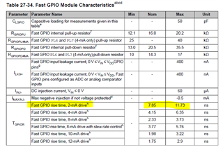
      There is no such external pin to accept a skewed clock. In high speed clock operation with HSCLKEN bit set to 1, the QSSI master clock is reflected back as a loopback clock, HSPEEDCLK, to the QSSI module. The HSPEEDCLK is used as the clock to sample the data from the slave. As you can see there is some I/O delay from the time the internal SPICLK is generated until it comes out on the I/O pad, this indirectly is acting as an intentional clock skew. In the datasheet, the 2ma I/O buffer delay can be up to 11.73ns at the max condition. Although much smaller, there is also an input buffer delay. What this means is that there is at least 11.73ns of delay between the internal clock to the  HSPEEDCLK clock sampling the data. This number is close to your IL715 delay. You also have half cycle of SPICLK before the sampling the data (e.g. master sending data on the rising edge and sampling data on the falling edge). Unless you are operating at extremely fast SPICLK baudrate, I think the high speed mode will be able to help you. I will suggest you start without the high speed mode first and do some measurement to see if you have sufficient time for the slave data to arrive before master's sampling edge. This will depend on the baudrate you choose.  If the timing is ok then there is no need for high speed mode. 

  • Hi Charles,

    thanks for an excellent answer. We are running the QSSI clock at 20MHz. The IL715 is running at 3V3 which give 12ns typical and 18ns max delay across the barrier so the even with HSPEEDCLK the communication would be pretty marginal. We are talking to a ADS1278 which is an 8 channel 24bit ADC with an audio synchronous serial like interface (also SPI, but we want sync serial for lower noise) so generating the frame sync pulse would be challenging too. It's time to have a hard look for another processor - ideally one where we can have some confidence of supply!