This thread has been locked.
If you have a related question, please click the "Ask a related question" button in the top right corner. The newly created question will be automatically linked to this question.
Hi Expert,
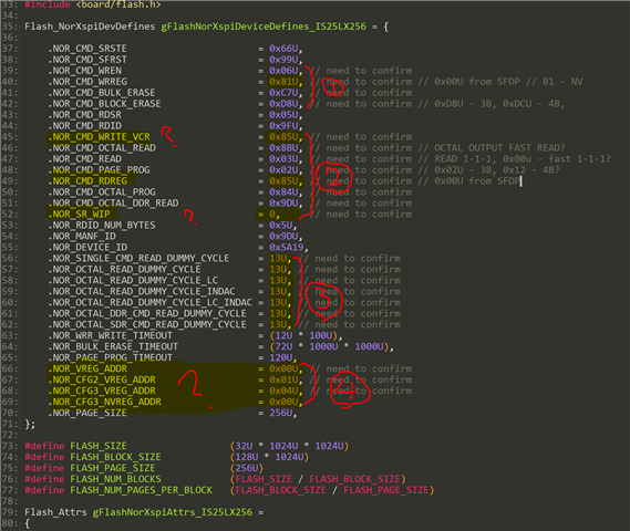
For the custom xSpi flash driver of "IS25LX256", I followed up the steps TI guided.
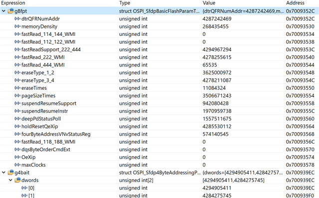
step 1, step2, and step 3 have been done without error. I was able to see SFDP information from the new flash using OSPI Flash Diagnostic and mapped it to the setting in the flash driver, and also enabled the new xSpi in syscfg as below.
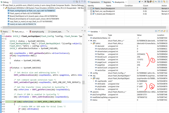
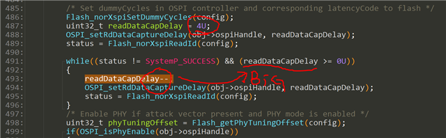
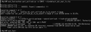
However, in step 4, when I executed OSPI Flash IO, the manufacturer ID and device ID were always 0x0 and 0x0 and stuck in Flash_norXspiReadId().
Flash_NorXspiDevDefines gFlashNorXspiDeviceDefines_IS25LX256 = { .NOR_CMD_SRSTE = 0x66U, .NOR_CMD_SFRST = 0x99U, .NOR_CMD_WREN = 0x06U, .NOR_CMD_WRREG = 0x00U, .NOR_CMD_BULK_ERASE = 0xC7U, .NOR_CMD_BLOCK_ERASE = 0xD8U, .NOR_CMD_RDSR = 0x05U, .NOR_CMD_RDID = 0x9FU, .NOR_CMD_WRITE_VCR = 0x85U, .NOR_CMD_OCTAL_READ = 0x7CU,//0x8BU, 4byte address .NOR_CMD_READ = 0x03U, .NOR_CMD_PAGE_PROG = 0x02U, .NOR_CMD_RDREG = 0x00U, .NOR_CMD_OCTAL_PROG = 0x84U, .NOR_CMD_OCTAL_DDR_READ = 0x9DU, .NOR_SR_WIP = 0, .NOR_RDID_NUM_BYTES = 0x5U, .NOR_MANF_ID = 0x9DU, .NOR_DEVICE_ID = 0x5A19, .NOR_SINGLE_CMD_READ_DUMMY_CYCLE = 0U, .NOR_OCTAL_READ_DUMMY_CYCLE = 8U, .NOR_OCTAL_READ_DUMMY_CYCLE_LC = 0x0U, .NOR_OCTAL_READ_DUMMY_CYCLE_INDAC = 0U, .NOR_OCTAL_READ_DUMMY_CYCLE_LC_INDAC = 0x0U, .NOR_OCTAL_DDR_CMD_READ_DUMMY_CYCLE = 8U, .NOR_OCTAL_SDR_CMD_READ_DUMMY_CYCLE = 0U, .NOR_WRR_WRITE_TIMEOUT = (12U * 100U), .NOR_BULK_ERASE_TIMEOUT = (72U * 1000U * 1000U), .NOR_PAGE_PROG_TIMEOUT = 12U, .NOR_VREG_ADDR = 0x000000U, .NOR_CFG2_VREG_ADDR = 0x000003U, .NOR_CFG3_VREG_ADDR = 0x000004U, .NOR_CFG3_NVREG_ADDR = 0x00U, .NOR_PAGE_SIZE = 256U, }; #define FLASH_SIZE (32U * 1024U * 1024U) #define FLASH_BLOCK_SIZE (128U * 1024U) #define FLASH_PAGE_SIZE (256U) #define FLASH_NUM_BLOCKS (FLASH_SIZE / FLASH_BLOCK_SIZE) #define FLASH_NUM_PAGES_PER_BLOCK (FLASH_BLOCK_SIZE / FLASH_PAGE_SIZE) Flash_Attrs gFlashNorXspiAttrs_IS25LX256 = { .deviceId = 0, /* filled by Flash_open, after querying the flash */ .manufacturerId = 0, /* filled by Flash_open, after querying the flash */ .driverInstance = 0, /* filled by SysConfig */ .flashSize = FLASH_SIZE, .blockCount = FLASH_NUM_BLOCKS, .blockSize = FLASH_BLOCK_SIZE, .pageCount = FLASH_NUM_PAGES_PER_BLOCK, .pageSize = FLASH_PAGE_SIZE, .sectorSize = 0, /* NOT USED */ .sectorCount = 0, /* NOT USED */ };
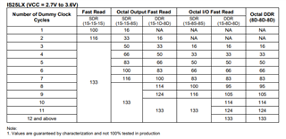
Q1) Could you share any checkpoints related to this problem? Should I customize the syscfg as well with the IS25LX256 datasheet, like input clock frequency, divider, DDR, PHY and so on?
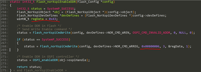
Q2) I found some hard code in Flash_norXspiEnableDDR() in "flash_not_xspit.c" in SDK as below. This seems to be the code for the infieon-specific xSPi flash used for TI evaluation board. Do I have to modify this function even though it is a common function executed for every xSpi flash?
I would appreciate it if you share your experience and knowledge on this custom flash driver issue as well.
Regards,
Moonil
Hi Moonil,
Apologies for such hiccups. This is to let you know that we are undergoing some changes to have better experience for flash driver. But for current version of SDK, I can extend some pointers for you -
1. The ospi_flash_diag is working on 1s-1s-1s mode whereas ospi_flash_io is functional in 8d-8d-8d mode, so it seems like the flash driver is functional for 1s-1s-1s mode but not for 8d-8d-8d mode. You also need to configure the dummy cycles to higher number.
2. When the PHY Mode is enabled, the Clock Divider is bypassed. So your driver is clock enabled for 200MHz, but the part number you shared does not support 200MHz. Can you lower your clock to 133MHz ?
Also, the flash_diag works on very slow clock which overrides the sysconfig in the code.
Accordingly, the dummy cycles will be 12-13.
3. Try disabling the PHY Mode for starters. It might just work with this too, then more tuning should be done in place.
Hope that helps.
Best Regards,
Aakash
Hi Aakash,
Thank you for your prompt support and also your review of the IS25LX256 datasheet.
I tried the configuration which you pointed out but the issue was still the same as before.
"flash_nor_xspi_device_IS25LX256.c":
/* * Copyright (C) 2021 Texas Instruments Incorporated * * Redistribution and use in source and binary forms, with or without * modification, are permitted provided that the following conditions * are met: * * Redistributions of source code must retain the above copyright * notice, this list of conditions and the following disclaimer. * * Redistributions in binary form must reproduce the above copyright * notice, this list of conditions and the following disclaimer in the * documentation and/or other materials provided with the * distribution. * * Neither the name of Texas Instruments Incorporated nor the names of * its contributors may be used to endorse or promote products derived * from this software without specific prior written permission. * * THIS SOFTWARE IS PROVIDED BY THE COPYRIGHT HOLDERS AND CONTRIBUTORS * "AS IS" AND ANY EXPRESS OR IMPLIED WARRANTIES, INCLUDING, BUT NOT * LIMITED TO, THE IMPLIED WARRANTIES OF MERCHANTABILITY AND FITNESS FOR * A PARTICULAR PURPOSE ARE DISCLAIMED. IN NO EVENT SHALL THE COPYRIGHT * OWNER OR CONTRIBUTORS BE LIABLE FOR ANY DIRECT, INDIRECT, INCIDENTAL, * SPECIAL, EXEMPLARY, OR CONSEQUENTIAL DAMAGES (INCLUDING, BUT NOT * LIMITED TO, PROCUREMENT OF SUBSTITUTE GOODS OR SERVICES, LOSS OF USE, * DATA, OR PROFITS, OR BUSINESS INTERRUPTION) HOWEVER CAUSED AND ON ANY * THEORY OF LIABILITY, WHETHER IN CONTRACT, STRICT LIABILITY, OR TORT * (INCLUDING NEGLIGENCE OR OTHERWISE) ARISING IN ANY WAY OUT OF THE USE * OF THIS SOFTWARE, EVEN IF ADVISED OF THE POSSIBILITY OF SUCH DAMAGE. */ #include <board/flash.h> Flash_NorXspiDevDefines gFlashNorXspiDeviceDefines_IS25LX256 = { .NOR_CMD_SRSTE = 0x66U, .NOR_CMD_SFRST = 0x99U, .NOR_CMD_WREN = 0x06U, // need to confirm .NOR_CMD_WRREG = 0x00U, // need to confirm .NOR_CMD_BULK_ERASE = 0xC7U, // need to confirm .NOR_CMD_BLOCK_ERASE = 0xD8U, // 0xD8U - 3B, 0xDCU - 4B, // need to confirm .NOR_CMD_RDSR = 0x05U, .NOR_CMD_RDID = 0x9FU, .NOR_CMD_WRITE_VCR = 0x85U, // need to confirm .NOR_CMD_OCTAL_READ = 0x8BU, // OCTAL OUTPUT FAST READ? need to confirm .NOR_CMD_READ = 0x03U, // READ 1-1-1, 0x00u - fast 1-1-1? need to confirm .NOR_CMD_PAGE_PROG = 0x02U, // 0x02U - 3B, 0x12 - 4B ? need to confirm .NOR_CMD_RDREG = 0x00U, // need to confirm .NOR_CMD_OCTAL_PROG = 0x84U, // need to confirm .NOR_CMD_OCTAL_DDR_READ = 0x9DU, // need to confirm .NOR_SR_WIP = 0, .NOR_RDID_NUM_BYTES = 0x5U, .NOR_MANF_ID = 0x9DU, .NOR_DEVICE_ID = 0x5A19, .NOR_SINGLE_CMD_READ_DUMMY_CYCLE = 13U, // need to confirm .NOR_OCTAL_READ_DUMMY_CYCLE = 13U, // need to confirm .NOR_OCTAL_READ_DUMMY_CYCLE_LC = 13U, // need to confirm .NOR_OCTAL_READ_DUMMY_CYCLE_INDAC = 13U, // need to confirm .NOR_OCTAL_READ_DUMMY_CYCLE_LC_INDAC = 13U, // need to confirm .NOR_OCTAL_DDR_CMD_READ_DUMMY_CYCLE = 13U, // need to confirm .NOR_OCTAL_SDR_CMD_READ_DUMMY_CYCLE = 13U, // need to confirm .NOR_WRR_WRITE_TIMEOUT = (12U * 100U), .NOR_BULK_ERASE_TIMEOUT = (72U * 1000U * 1000U), .NOR_PAGE_PROG_TIMEOUT = 120U, //12U .NOR_VREG_ADDR = 0x0U, // volatile register address is correct? .NOR_CFG2_VREG_ADDR = 0x01U, // volatile register for dummy cycle? correct? .NOR_CFG3_VREG_ADDR = 0x04U, // what address should be for this? .NOR_CFG3_NVREG_ADDR = 0x00U, .NOR_PAGE_SIZE = 256U, }; #define FLASH_SIZE (32U * 1024U * 1024U) #define FLASH_BLOCK_SIZE (128U * 1024U) #define FLASH_PAGE_SIZE (256U) #define FLASH_NUM_BLOCKS (FLASH_SIZE / FLASH_BLOCK_SIZE) #define FLASH_NUM_PAGES_PER_BLOCK (FLASH_BLOCK_SIZE / FLASH_PAGE_SIZE) Flash_Attrs gFlashNorXspiAttrs_IS25LX256 = { .deviceId = 0, /* filled by Flash_open, after querying the flash */ .manufacturerId = 0, /* filled by Flash_open, after querying the flash */ .driverInstance = 0, /* filled by SysConfig */ .flashSize = FLASH_SIZE, .blockCount = FLASH_NUM_BLOCKS, .blockSize = FLASH_BLOCK_SIZE, .pageCount = FLASH_NUM_PAGES_PER_BLOCK, .pageSize = FLASH_PAGE_SIZE, .sectorSize = 0, /* NOT USED */ .sectorCount = 0, /* NOT USED */ };
"example.syscfg":
I captured the applied setting when Flash_norXspiOpen() was called, as below. they seemed to be correctly set.
Q1) Is there another check-point for this problem? I would like to review with you again about the commands, register address and dummy cycles mapped in "flash_nor_xspi_device_IS25LX256.c", SFDP from TI ospi_flash_diag below, and IS25LX256 datasheet. Could you review these? Please find SFDP below and c file above in this post. For example, XSPI_NOR_CMD_WRREG = 0x00 in SFDP, but I found the datasheet mention 81h for non-volatile register write. I would like to cross-check those with you.
"SFDP" from TI ospi_flash_diag:
[OSPI Flash Diagnostic Test] Starting ... [OSPI Flash Diagnostic Test] Flash Manufacturer ID : 0x9D [OSPI Flash Diagnostic Test] Flash Device ID : 0x5A19 [OSPI Flash Diagnostic Test] Executing Flash Erase on first block... [OSPI Flash Diagnostic Test] Done !!! [OSPI Flash Diagnostic Test] Performing Write-Read Test... [OSPI Flash Diagnostic Test] Write-Read Test Passed! [OSPI Flash Diagnostic Test] SFDP Information : ================================================ SFDP ================================================ SFDP Major Revision : 0x1 SFDP Minor Revision : 0x6 Number of Parameter Headers in this Table : 2 Types of Additional Parameter Tables in this flash --------------------------------------------------- 4 BYTE ADDRESSING MODE INSTRUCTIONS TABLE Flash_NorXspiDevDefines gFlashNorXspiDeviceDefines_<part-number> = { .XSPI_NOR_CMD_RSTEN = 0x66, .XSPI_NOR_CMD_RSTMEM = 0x99, .XSPI_NOR_CMD_WREN = 0x06, .XSPI_NOR_CMD_WRREG = 0x00, .XSPI_NOR_CMD_BULK_ERASE = 0xC7, .XSPI_NOR_CMD_SECTOR_ERASE_3B = 0x20, .XSPI_NOR_CMD_SECTOR_ERASE_4B = 0x21, .XSPI_NOR_CMD_BLOCK_ERASE_3B = 0xD8, .XSPI_NOR_CMD_BLOCK_ERASE_4B = 0xDC, .XSPI_NOR_CMD_PAGE_PROG_3B = 0x02, .XSPI_NOR_CMD_PAGE_PROG_4B = 0x12, .XSPI_NOR_CMD_RDSR = 0x05, .XSPI_NOR_CMD_RDREG = 0x00, .XSPI_NOR_CMD_RDID = 0x9F, .XSPI_NOR_CMD_READ = 0x03, .XSPI_NOR_CMD_888_SDR_READ = 0x00, .XSPI_NOR_CMD_888_DDR_READ = 0x00, .XSPI_NOR_CMD_444_SDR_READ = 0x00, .XSPI_NOR_CMD_444_DDR_READ = 0x00, .XSPI_NOR_CMD_114_READ = 0x00, .XSPI_NOR_SR_WIP = 0, .XSPI_NOR_SR_WEL = 0, .XSPI_NOR_RDID_NUM_BYTES = 5, .XSPI_NOR_MANF_ID = 0x9D, .XSPI_NOR_DEVICE_ID = 0x5A19, .XSPI_NOR_114_READ_MODE_CLKS = 0, .XSPI_NOR_114_READ_DUMMY_CYCLES = 0, .XSPI_NOR_444_READ_MODE_CLKS = 0, .XSPI_NOR_444_READ_DUMMY_CYCLES = 0, .XSPI_NOR_444_READ_DUMMY_CYCLES_LC = 0x00, .XSPI_NOR_QUAD_CMD_READ_DUMMY_CYCLES = 0x00, .XSPI_NOR_OCTAL_READ_DUMMY_CYCLE = 0, .XSPI_NOR_OCTAL_READ_DUMMY_CYCLE_LC = 0x00, .XSPI_NOR_OCTAL_DDR_RDSR_DUMMY_CYCLE = 0, .XSPI_NOR_OCTAL_DDR_RDREG_ADDR_BYTES = 0, .XSPI_NOR_OCTAL_DDR_WRREG_ADDR_BYTES = 0, .XSPI_NOR_OCTAL_DDR_RDVREG_DUMMY_CYCLE = 0, .XSPI_NOR_OCTAL_DDR_RDNVREG_DUMMY_CYCLE = 0, .XSPI_NOR_OCTAL_RDSFDP_DUMMY_CYCLE = 0, .XSPI_NOR_OCTAL_RDSFDP_ADDR_TYPE = 0, .XSPI_NOR_WRR_WRITE_TIMEOUT = 1200, .XSPI_NOR_BULK_ERASE_TIMEOUT = 72000000, .XSPI_NOR_PAGE_PROG_TIMEOUT = 120, .XSPI_NOR_VREG_OFFSET = 0x0, .XSPI_NOR_NVREG_OFFSET = 0x0, .XSPI_NOR_QUAD_MODE_CFG_ADDR = 0x0, .XSPI_NOR_QUAD_MODE_CFG_BIT_LOCATION = 0x0, .XSPI_NOR_DDR_OCTAL_MODE_CFG_ADDR = 0x0, .XSPI_NOR_DDR_OCTAL_MODE_CFG_BIT_LOCATION = 0x0, .XSPI_NOR_DUMMY_CYCLE_CFG_ADDR = 0x0, .XSPI_NOR_FLASH_SIZE = 33554432, .XSPI_NOR_PAGE_SIZE = 256, .XSPI_NOR_BLOCK_SIZE = 131072, .XSPI_NOR_SECTOR_SIZE = 4096, .addrByteSupport = 1, .dtrSupport = 1, .qeType = 7, .seq444Enable = { 0, 0, 0, 0, 0 }, .seq444Disable = { 0, 0, 0, 0 }, .oeType = 0, .cmdExtType = 0, .byteOrder = 0, }; All tests have passed!!
Q2) I still want to check with you about the previous question (Q2) in my first post. I found "Flash_norXspiEnableDDR()" has some hard codes for Infineon flash embedded in TI evaluation board. In this function, "regData" is 0x43, and cmd address is 0x00800006 as you can see in the code below. This function is called by Flash_open() if dtr is enabled. Do you think this hard code can be related to the current issue for IS25LX256 flash? if yes, could you guide me on how to change this function?
Regards,
Moonil
Hi Moonil,
Yes you're right, the current driver function has some hardcoding for the spansion flash. I took a look at the datasheet of the ISSI flash you're using, and seems like for enabling Octal DDR, the bit pattern to be written is 0xE7, to volatile configuration register with address 0x00. Command to write the volatile register is 0x81, and to read would be 0x85. In this function, I think you would have to change
```
regData = 0xE7;
```
AND
```
status = Flash_norXspiCmdWrite(config, 0x81, 0x00, 3, ®Data, 1);
```
and rest of the things same. Make sure that after Octal DDR is enabled, everything in controller also should be setup to use this protocol, as in setting the lines, address bytes etc. Let me know if there is any progress after this. You would need to set the right dummy cycles and adjust the RD DATA CAPTURE DELAY also correctly for the reads to work properly. (this should already be part of the driver)
Regards,
Anand M
Moonil,
I want to request for one more piece of data if possible, can you run the ospi_flash_diag again and capture the values of variables gBfpt (of type NorSpi_SfdpBasicFlashParamTable) and g4bait (of type NorSpi_Sfdp4ByteAddressingParamTable) and send here either as a binary dump or text? I am interested in how the octal DDR information is provided in the table.
Regards,
Anand M
Hi Anand,
Thank you for your prompt response with very details.
Yes you're right, the current driver function has some hardcoding for the spansion flash. I took a look at the datasheet of the ISSI flash you're using, and seems like for enabling Octal DDR, the bit pattern to be written is 0xE7, to volatile configuration register with address 0x00. Command to write the volatile register is 0x81, and to read would be 0x85. In this function, I think you would have to change
```
regData = 0xE7;
```
AND
```
status = Flash_norXspiCmdWrite(config, 0x81, 0x00, 3, ®Data, 1);
When I tried the same test with "regData = 0xE7" and "status = Flash_norXspiCmdWrite(config, 0x81, 0x00, 3, ®Data, 1);" as you commented, I was able to see different values like 0x01 and 0xff00 instead of 0x00. But, it still failed to read the correct ID.
Q1) I also updated gFlashNorXspiDeviceDefines_IS25LX256 as below as you pointed out about read/write registers, but some parameters are still questionable to me. Could you please review this table and correct any wrong parameters?
You would need to set the right dummy cycles and adjust the RD DATA CAPTURE DELAY also correctly for the reads to work properly. (this should already be part of the driver)
Q2) for "RD DATA CAPTURE DELAY", I found the value is 4U in the existing TI code as below, however, this value becomes a big value after a few minus operation because its data type is unsigned type (uint32). This leads to almost infinite loops of the "while" when failing to read ID. Should we fix this as well? and 4U is correct for "readDataCapDelay" of IS25LX256?
I want to request for one more piece of data if possible, can you run the ospi_flash_diag again and capture the values of variables gBfpt (of type NorSpi_SfdpBasicFlashParamTable) and g4bait (of type NorSpi_Sfdp4ByteAddressingParamTable) and send here either as a binary dump or text? I am interested in how the octal DDR information is provided in the table.
Please find the dump files for gBfpt and g4bait below, and also refer to the captured image from ccs.
/cfs-file/__key/communityserver-discussions-components-files/908/gBfpt.dat
/cfs-file/__key/communityserver-discussions-components-files/908/g4bait.dat
Regards,
Moonil
Hi Moonil,
Thanks for the due diligence. I will need one more day to parse the 4 byte addressing table and BFPT data. Meanwhile I can answer Q1 and Q2.
Q1
1) RDREG and WRREG parsing is incorrect in the SDK version you're using. This will be fixed in a newer SDK. 0x81 and 0x85 are the correct values.
2) NOR_SR_WIP should be (1 << 0), again the ospi_flash_diag doesn't print the "1 << " part (bug which is fixed now) so it seems incorrect. You should update the value as (1 << 0) or simply 1.
3) Dummy Cycles matter only in read, and read is done only in DAC mode. I think the fields which will matter are
NOR_OCTAL_READ_DUMMY_CYCLE NOR_OCTAL_READ_DUMMY_CYCLE_LC NOR_OCTAL_DDR_CMD_READ_DUMMY_CYCLE NOR_SINGLE_CMD_READ_DUMMY_CYCLE
Hi Anand M,
I will need one more day to parse the 4 byte addressing table and BFPT data
Thanks for your feedback again and let me wait for your review of BFPT data.
You're right, that is a bug which might put it into infiinte loop if it's not able to read the ID using any of the values from 4 to 1. The bug is fixed in newer SDKs. But if it doesn't find a value within those, then there is some other issue as well. You can try looping from 8 through 0 and change the >= to a >
SDK version 08.00.02.31 is used for our project. yes, I found this fix in 08.00.03.18 but other logic in driver is same. so I think SDK version will not resolve out current issue. please let me know if we need to update SDK with the latest version.
2) NOR_SR_WIP should be (1 << 0), again the ospi_flash_diag doesn't print the "1 << " part (bug which is fixed now) so it seems incorrect. You should update the value as (1 << 0) or simply 1.
I tested the same after all change and fix we discussed. but still failed to read ID with them.
so, I also checked some pin signals like spi0_clk, DQ0 and DQ7, using "ospi_flash_daig" and "ospi_flash_io" as below.
1) ospi_flash_daig (1-1-1 mode): it looks good.
2) "ospi_flash_io" (8-8-8 mode): it looks a bit weird to me.
Do you think the signal of DQ0 and DQ07 below is problematic? if yes, is this signal related to the parameters set we are discussing?
FYI, these signals were captured during the code execution (1) below.
I would appreciate it if you share the result of your review BFPT data and your opinion on my question above.
I think we can also have a call in one or two days to investigate this issue together on my real target. (with sharing my screen using MS Teams). Please let me know when you are available.
Regards,
Moonil
Hi Anand,
Could you let me know if there is any update on this topic at your end?
Regards,
Moonil
Hi Anand,
As we discussed in the debug session, Octal DDR is not working now and so 1s-1s-1s can be a choice for our urgent dev schedule if its speed is not that slow for bootup.
So, I tested 1s-1s-1s mode with "ospi_flash_io" example on the evaluation board (AM2434 EVM). but assert happened as below,
Q1) Could you run opsi_flash_io and reproduce this with 1s-1s-1s mode on evm at your end, and clarify the reason why the assert happen?
I did test the same on the boot modes as below,
Q2) I also built/tested SBL_OSPI with enabling 1s-1s-1s mode on evm, SBL is not working as well. Do you think this is caused by the same reason as Q1 or any hw configuration fixed to Octal DDR mode in EVM?
As we know, we have to rebuild SBL OSPI with 1s-1s-1s mode for our product now. So this issue needs to be clarified urgently.
I am looking for your reply.
Regards
Moonil
Hi Moonil,
All the experts in India are OOO and will be back by Thursday. Apologies for the delay. We will get back to you ASAP.
Thanks and Regards,
Aakash
Hi Aakash,
Thanks for the information again.
Could you please arrange 3rd debug session on Thursday? In this session, we should focus on only 1s-1s-1s mode operation on SBL with EVM and real board.
Please send me the invitation for this meeting. the same time should be okay.
Regards,
Moonil
Hi Anand and Askash,
I tested 1s-1s-1s mode using applications on our real board as below,
So, it is unclear to me yet the reason why uart_uniflash is not working even though it used the same board.lib and syscfg used in ospi_flash_io.
I am wondering if we can trace the code of uart_uniflash app in CCS. Do we need CCS JS for sbl_ospi or uart_uniflash app debugging in CCS? if yes, could you please prepare JS for 3rd debugging session? I would like to check the code of uart_unifalsh in CCS together.
Thanks
Moonil
Hi Moonil,
How are you sure that UART_UNIFLASH is not working.. This seems to me like the Uart UniFlash has not yet started because ROM rejected your sbl_uart_uniflash image. Can you check which OpenSSL version are you using ? Is it OpenSSL 1.1.1k ?
The major difference in SBL Uart UniFlash and SBL Jtag UniFlash is that SBL Jtag Uniflash loads the .out file directly via debug access and does not require ROM to validate that SBL image (which is .tiimage format and a x509 format). Although for your AM243x, it is a GP device and ROM verification should not be mandatory.
Can you also put the device in UART BOOT mode and send a .tiimage via xmodem for SBL NULL ? Do you see any prints in that case ? Can you connect the debugger to R5 core and let us know what is the PC of that core ?
Best Regards,
Aakash
Hi Aakash,
This issue seems to be related to MMCSD in syscfg of uart_uniflash. after I modifed code, syscfg and library as below, it was fixed.
please let me know if my fix will harm any operation.
After this fix, uart_uniflash is working. But I found that it sometimes fails to flash images like the log below.
Once this failure happened, uart_uniflash was not able to flash images on that area anymore. Only after erasing all by using "jtag_uniflash", it was recovered.
Do you think this can be caused by flash driver configuration in "flash_nor_xspi_device_IS25LX256.c" or our change on "flash_nor_xspi.c" for 1s-1s-1s mode? Do we need to increase a timeout parameter?
Good thing is, today I was able to create sbl with 1s-1s-1s mode and make the system bootup with SPI boot mode on our real board. However, this flash failure seems to happen quite frequently ( 1 failure per 5 tests ) when using uart_uniflash.
Q1) Could you please share any checkpoints on this flash failure?
Q2) Can we add a flash erase command in uart_uniflash to recover this failure like jtag_uniflash? (like modifying cfg file.) because jtag will not be used in our firmware upgrade process.
Regards,
Moonil
Hi Moonil,
As discussed over call, this turns out to be a flash erase failure. This may be due to 4B addressing is being used in flash even though the flash is configured for 3B (default) mode. One suggestion would be to fix it to 3B in Flash Erase parameter.
I am not closing this thread and waiting for your response on the same.
BR,
Aakash
Hi Aakask and Anand
Thank you so much for your technical support. 1s-1s-1s mode is working well without flash erase failure in my test. I think we can close this post. However, we need to continue to debug the Octal DDR issue. For this, I sent a separate email to your team. Please reply to the email. Thanks again!