This thread has been locked.

If you have a related question, please click the "Ask a related question" button in the top right corner. The newly created question will be automatically linked to this question.

AM2634: ADC Sampling Priority of High-Priority vs RoundRobin (Measurements on the AM2634-CC V1)

Part Number: AM2634

Hi,

I do have a configuration where, one ADC is being triggered by two different trigger sources. I call them fs1 and fs3. fs1 being 200KHz and fs3 being 1KHz. The source of the triggers are ePWM untis. The input channels of the ADC are used in the following configuration:

I do apply a SINE WAVE on the CHx inputs and put the converted result back using DMA and the on chip DAC. This works perfect most of the time for all times except channel Ch0. I do use 3 EPWM units to create the triggers (fs1, fs2, fs3) that the ADC's are using. ADC0 shown above is using fs1 to convert the analong input on channel Ch0..Ch2. fs3 is used to convert the remaining channels. Each 1 ms fs1 and fs3 to happen at the very same moment in time - well that's what I assume. The scope shot for the trigger looks the following:

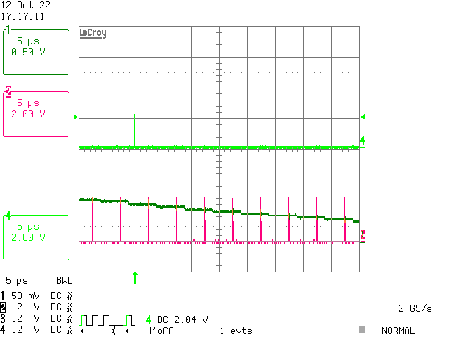
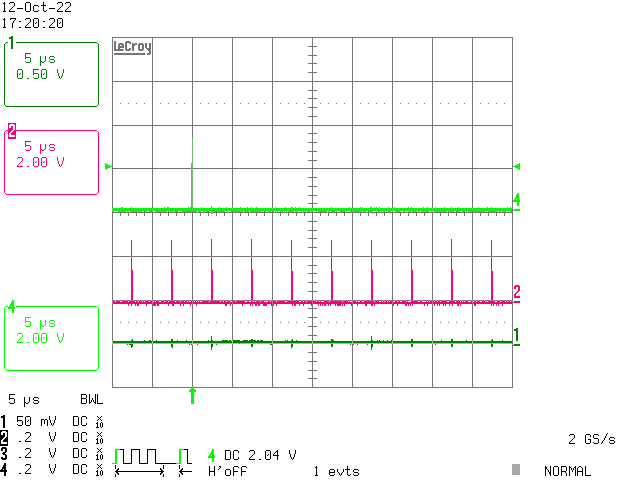
On this shot the input and the three triggers are shown. The triggers are brought to pins in order to capture them as well.

Ch1 --> DAC output

Ch2 --> fs1 (200 KHz)

Ch3 --> fs2 (50 KHz)

Ch4 --> fs3 ( 1 KHz)

As said it works fine most of the except for channel Ch0 of the ADC if fs3 and fs1 do occurr at the same time.  The configuration of the ADC trigger is made such that Ch0..Ch2 are in "high priority trigger mode" while channel Ch3..Ch5 are used in the RoundRobin trigger mode.

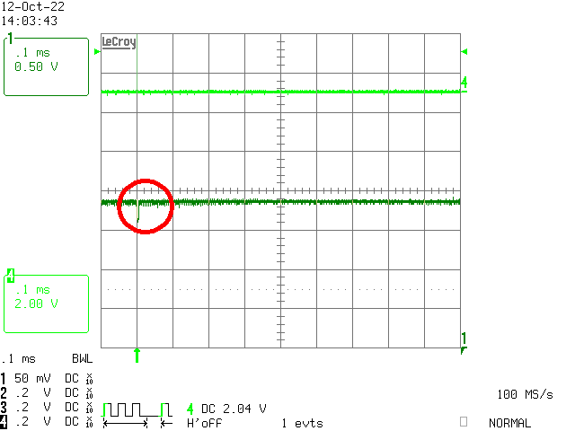
Looking closer to the DAC output with a slow moing input sine being sampled I do discover a peak or a glitch a do not see for all the other channels being brought to the DAC port. Even if I do remove the sine from Ch0 an short it I do get this glitch then and only then if fs1 and fs3 do happen at the very same time.

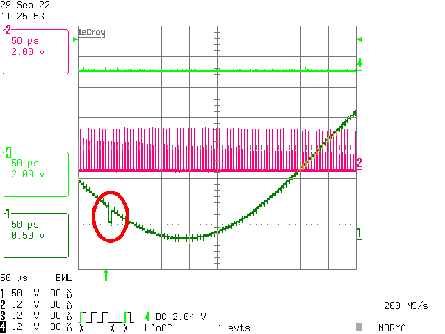
The scope shot does show the sine input signal on Ch0 while fs1 and fs3 do happen at the very same moment in time. I do assume it has something to do internally with the trigger priority of the ADC0. Now comes the question

Q: Is there a way I can easily delay the occurrence of fs3 (sourced by an ePWM unit) by lets say 1 usec or so with respect to fs1 (200 KHz) such that it still is 1KHz sampling but guaranteed to happen always 1usec later than fs1?

My assumption is that then it works as expected even for the input Ch0. Because I do never see this behavior for the inputs Ch1 or Ch2 of ADC0 which are converted only a few hundred ns later than Ch0. I do assume maybe a configuration issue for the ePWM units or for the ADC trigger or an internal problem between high-priority trigger and round robin trigger of the ADC itself. I don't know. According to the documentation the 'high-priority-trigger' should win vs the RoundRobin trigger if the triggers do occur within the same clock cycle.

br

Markus

  • As an additional info I did play around with the startvalue of the ePWM untis in the TimeBase section within SysCfg. This way I can shift in phase of the three triggers with respect to each other. However I get the impression it has to do with the input channel Ch0 only. May be it is a layout or a pin assignment thing. Anyway I changed from ADC0 to ADC1 and to the input pins for the ADC1. Again on the input channel Ch0 I get this peaking. At the moment I don't now what to do. For our application we need all of the channels for different inputs. Otherwise one could just sacrify one analog input. But for the moment I would like to understand why I do get this on the input Ch0. Ch0 is the first one being converted after a SOC_A/B trigger.

    Here Ch0 ADC0 has a DC input only. No sine wave input. However at the moment the 1KHz trigger appears the converted Ch0 has this disturbance shown above. Ch0 is being triggered by the 200KHz trigger and not by the 1KHz trigger. Scope Channel Ch4 shows the 1ms triggers fs3.

    The ADCx has been configured such that is asserts the interrupt after the conversion of the first channel being converted. Maybe for some kind of reason the interrupt appears to early the conversion is completed completely and the DMA reads a value close to the final value but not the final one. The pulse shown above is moving with the input signal. It is not a complete different value.

    Changing from Ch0 to CH1 or other channel the problem dissapears. It looks like it has to do with internal timing sequence in some way. If TI support requires the project, please drop me a private email. I can not post the test project into e2e, since it is work for a customer.

  • Some additional info. Now I did move fs3 (1KHz) trigger for the channels 3..5 on ADC0 in between two fs1 triggers. fs1 is 200 KHz. I assume that there is some idle time between the conversion of Ch0..Ch2 and Ch3..Ch5. As a reminder the input signal we are watching here is 1KHz Sine Input with a Vpp of ~3Volt. An offset of 1.5V has been set on the function generator to 'place' the input signal somewhat optimal for the ADC's analog input signal range. It is assumed this is between 0..~3V

    Still the peak exist with some informational findings:

    Scope CH4 fs3 1KHz in between two fs1 SOC triggers
    Scope CH2 fs1 200 KHz
    Scope CH1 the DAC output of the digitized input CH0 of ADC0

    In about the middle of the input ~1.5V there is not much of an influence. Near the maximum of the analog input range it looks the following:
    The input value or the 'charge' being added looks positive...

    Near the 0V input range it looks the following:

    The input value or the charge been added looks 'negative'. Again if I do switch to ADC0-CH1 which is sampled with the same fs1 200 KHz there is nothing to see. Next I will try to 'double sample' CH0 wasting a little bit of ADC's sampling bandwidth and see if the 2nd conversion is influenced or not. The ADC's interrupt that is triggering the DMA transfer will be set to the last channel making sure we have stable values in the SOC's result registers.

  • As a final note for today. If I do the following and the problem mostly disappears. Still I would be happy if an expert on TI's side or any other expert that is familiar with this type of Soc can have a look inside.

    I do the following:

    Added one additional SOC at the very beginning. Basically I do double sample CH0 and use the second one. Still fs3 is in between two consequtive fs1. If not the problem is still there. ThereforeI need to apply both 'workarounds' on my project. It is still possible that the root cause is my configuration, I don't know yet. Therefore an experts comment is welcome.

    This concept does cost a little bit of sampling banswitdh. However in the customers context it is still ok. Since it is not 100% gone, but lets say 95% I would like to understand the root cause.

    No artefact is 'seen' near the fs3 1KHz sample puls.

    fs3 is being placed in between two consequtive fs1 triggers.

    fs1 triggers Ch0-Ch0-Ch1-Ch2 in high priority mode
    fs3 triggers Ch3-Ch4-Ch5 in RoundRobin mode

    No artefact is seen.

    The analog input Ch0 of ADC0 is grounded, Nothing is seen.

    The analog input is left open. I know this is not realistic szenario. However it shows that still some 'charge' is being coupled into the ADC system. Root cause unknown. There is maybe even a requirement to drive the input and to not them left open which I have no problems with it.

    br

    Markus

  • Hi Markus

    Looking into this, will get back to you shortly

    Thanks & Regards
    Sri Vidya

  • Hi Markus,

    If TI support requires the project, please drop me a private email. I can not post the test project into e2e, since it is work for a customer.

    I think this would help since the SW/HW configuration is complex (EPWM,ADC,EDMA,DAC). I'll send you an email.

    I've looped in ADC experts from HW teams for additional comment.

    Regards,
    Frank

  • Hi Frank, I will prepare everything for Monday