This thread has been locked.

If you have a related question, please click the "Ask a related question" button in the top right corner. The newly created question will be automatically linked to this question.

RM57L843: How does the HET module generate pulse signals with different phase shifts?

Part Number: RM57L843
Other Parts Discussed in Thread: HALCOGEN

Hi team,

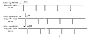
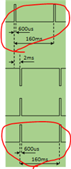
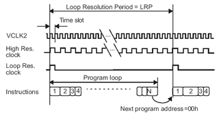
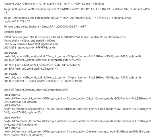
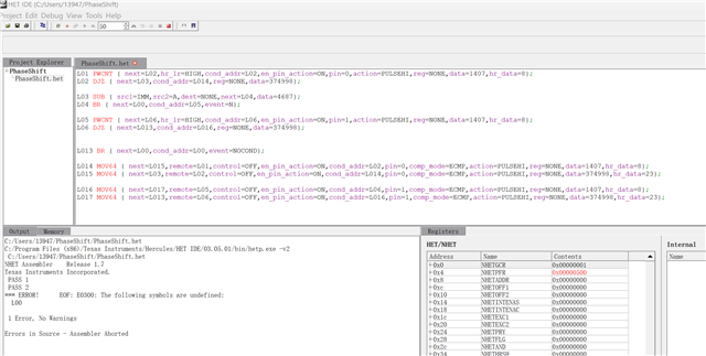
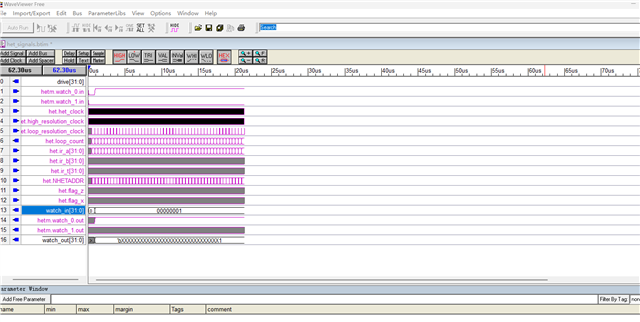
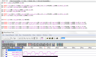
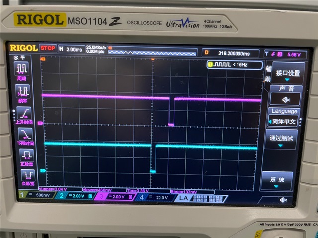
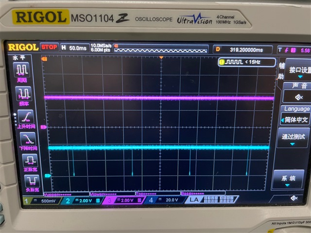
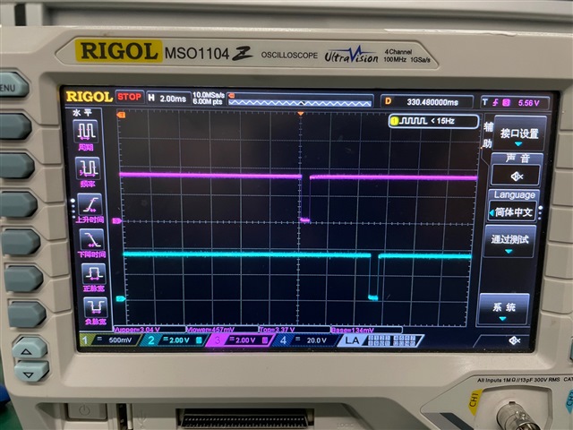
The N2HET module can generate pulse signals with different duty cycles, the customer would like to know how can different phase shift be applied to these pulse signals? 

Thanks.

Best Regards,

Cherry

  • the customer would like to know how can different phase shift be applied to these pulse signals? 

    Does the "phase shift" here mean the dead-band between two PWM signals?

  • Hi,

    Thanks for your support.

    If the phase shift is different between the two pulse signals and the period and duty cycle are the same, the waveform is the same just with a delay. The final output waveform can only be determined if the period, duty cycle, and phase shift are all defined. 

    Thanks and regards,

    Cherry

  • Yes, you can do it with N2HET assembly instructions. I will give you an example for shifting the 2nd PWM pulse.

  • This is an example:

    ====================

    L00 CNT { reg=A,max=0x1FFFFFF,data=0};

    L01 PWCNT { next=L02,cond_addr=L02,en_pin_action=ON,pin=0,action=PULSEHI,reg=NONE,data=5};
    L02 DJZ { next=L03,cond_addr=L014,reg=NONE};

    L03 SUB { src1=IMM,src2=A,dest=NONE,next=L04,data=7};
    L04 BR { next=L00,cond_addr=L05,event=N};

    L05 PWCNT { next=L06,cond_addr=L06,en_pin_action=ON,pin=1,action=PULSEHI,reg=NONE,data=5};
    L06 DJZ { next=L013,cond_addr=L016,reg=NONE};


    L013 BR { next=L00,cond_addr=L00,event=NOCOND};

    L014 MOV64 { next=L015,remote=L01,control=OFF,en_pin_action=ON,cond_addr=L02,pin=0,comp_mode=ECMP,action=PULSEHI,reg=NONE,data=5,hr_data=2};
    L015 MOV64 { next=L03,remote=L02,control=OFF,en_pin_action=ON,cond_addr=L014,pin=0,comp_mode=ECMP,action=PULSEHI,reg=NONE,data=9,hr_data=2};

    L016 MOV64 { next=L017,remote=L05,control=OFF,en_pin_action=ON,cond_addr=L06,pin=1,comp_mode=ECMP,action=PULSEHI,reg=NONE,data=5,hr_data=2};
    L017 MOV64 { next=L013,remote=L06,control=OFF,en_pin_action=ON,cond_addr=L016,pin=1,comp_mode=ECMP,action=PULSEHI,reg=NONE,data=9,hr_data=2};

    ======================

    The PWM signal is generated using PWCNT and DJZ instructions. 

    MOV64 is to update the data and control of PWCNT and DJZ

    SUB and BR are used to insert delay before first PWM and 2nd PWM. 

  • Hi,

    Thanks for your help again.

    The customer also would like to know is there any doc could specify at what the parameters in the following instructions mean? And how each instruction maps to the address of hetRAM? So that they know how to write the program, control, and data of the corresponding instruction to the specific address.

    Could you help by using the following two columns of pulses as an example:

    1. Period 160ms, duty cycle 0.375%, delay 0ms;
    2. Period 160ms, duty cycle 0.375%, delay 2ms.

    Thanks and regards,

    Cherry

  • Hi Cherry,

    For pulse width, 600us in your case, please read the description of the instruction of PWCNT. The data and hr_data fields of PWCNT define the width of the pulse. In my example code,  Pulse Width = (PWCNT data - 1) * LRP 

    The data filed of DJZ instruction specifies the length of the period. In my example, Period = (DJZ Data + 1) * LRP

    The delay between two waveform = (SUB Data) * LRP

  • Assume VCLK=75MHz, hr_lr=0, hr=1, and lr=32, -->LRP = 1*32*13.33ns = 426.67ns

    To get 600us pulse width, the data register of PWCNT = 600*1000/426.67+1 = 1407.24  --> data=1407, hr_data=0.24*32 = 8

    To get 160ms period, the data register of DJZ = 160*1000*1000/426.67-1 = 374998.71 --> data=374998, hr_data=0.71*32 = 23

    To have 2 ms delay, SubData = 2ms/LRP = 2000000/426.67 = 4687

    Example code:

    ;PWM code for given HCLK frequency = 150MHz, VCLK2=75MHz, hr=1, and lr=32, so LRP=426.67ns
    ;Pulse Width = 600us, and period = 160ms
    ;The delay between two PWM signals is 2ms
    L00 CNT { reg=A,max=0x1FFFFFF,data=0};

    L01 PWCNT { next=L02,hr_lr=HIGH,cond_addr=L02,en_pin_action=ON,pin=0,action=PULSEHI,reg=NONE,data=1407,hr_data=8};
    L02 DJZ { next=L03,cond_addr=L014,reg=NONE,data=374998};

    L03 SUB { src1=IMM,src2=A,dest=NONE,next=L04,data=4687};
    L04 BR { next=L00,cond_addr=L05,event=N};

    L05 PWCNT { next=L06,hr_lr=HIGH,cond_addr=L06,en_pin_action=ON,pin=1,action=PULSEHI,reg=NONE,data=1407,hr_data=8};
    L06 DJZ { next=L013,cond_addr=L016,reg=NONE,data=374998};


    L013 BR { next=L00,cond_addr=L00,event=NOCOND};

    L014 MOV64 { next=L015,remote=L01,control=OFF,en_pin_action=ON,cond_addr=L02,pin=0,comp_mode=ECMP,action=PULSEHI,reg=NONE,data=1407,hr_data=8};
    L015 MOV64 { next=L03,remote=L02,control=OFF,en_pin_action=ON,cond_addr=L014,pin=0,comp_mode=ECMP,action=PULSEHI,reg=NONE,data=374998,hr_data=23};

    L016 MOV64 { next=L017,remote=L05,control=OFF,en_pin_action=ON,cond_addr=L06,pin=1,comp_mode=ECMP,action=PULSEHI,reg=NONE,data=1407,hr_data=8};
    L017 MOV64 { next=L013,remote=L06,control=OFF,en_pin_action=ON,cond_addr=L016,pin=1,comp_mode=ECMP,action=PULSEHI,reg=NONE,data=374998,hr_data=23};

  • Hi,

    Thanks for your response again!

    The customer has 2 more questions:

    1) Next program address is the RAM address of the next instruction. So what does the Conditional address mean, when or what conditions are met before the instruction pointed to by the Conditional address is executed, and if the instruction on the Conditional address is executed, Does the specified Next program address not execute?

    2) LRP is the key to calculating the data register duty, period, and delay values for MOV64 and sub. So what does LRP mean by LR, hr, and VCLK, respectively? How to confirm the actual VCLK, LR, and hr of the chip?

    Thanks and regards,

    Cherry

  • Hi Cherry,

    1. Next address is the next program address of the next instruction in the program flow. 

       Conditional address is the address of the next instruction when the condition occurs. The condition may be "equal to zero" or "Negative" or "falling edge". It is based on the instruction.

    L01 PWCNT { next=L02,hr_lr=HIGH,cond_addr=L02,en_pin_action=ON,pin=0,action=PULSEHI,reg=NONE,data=1407,hr_data=8};
    L02 DJZ { next=L03,cond_addr=L014,reg=NONE,data=374998};

    In DJZ instruction, the condition is when the data field decrements to zero. 

    L03 SUB { src1=IMM,src2=A,dest=NONE,next=L04,data=4687};
    L04 BR { next=L00,cond_addr=L05,event=N};

    In SUB instruction, the condition is event=Negative. 

    The  FLAGS Generated by Instruction are listed in one table in HET instruction section.

    2) LRP is the key to calculating the data register duty, period, and delay values for MOV64 and sub. So what does LRP mean by LR, hr, and VCLK, respectively? How to confirm the actual VCLK, LR, and hr of the chip?

    All N2HET timings are derived from VCLK2 which is one of the peripheral clocks. VCLK is the primary peripheral clock frequency, and VCLK2 and VCLK3 are the secondary peripheral clock frequency. HCLK is the system clock frequency, and GCLK is the CPU clock frequency. 

    hr: high resolution prescale factor (1, 2, 3, 4,..., 63, 64)                ---> HETPFR[5:0]
    lr: loop resolution prescale factor (1, 2, 4, 8, 16, 32, 64,128)        --->HETPFR[10:8] 
    HRP = high resolution clock period HRP = hr × TVCLK2 (ns)
    LRP = loop resolution clock period LRP = lr × HRP (ns)

    GCLK is =PLL clock if PLL is used as the clock source

    HCLK = GCLK/2, 3, ...  Maximum HCLK is 150MHz

    VCLK = HCLK/1,2.3...   Maximum VCLK is 110MHz

  • Hi,

    Thanks for your detailed answer.

    The following are two HETs of the RM57L843 chip that output pulse signals of the same period and duty cycle, one for PIN4 output of HET1 and the other for PIN3 output of HET2. The customer needs to increase PIN3 output of HET2 by 10ms over PIN4 output of HET1. 

    1) If PIN3 and PIN4 are on the same HET, simply add the SUB/BR operation between PWCNT/DJZ of PIN4 and PWCNT/DJZ of PIN3, as shown in the figure below, correct? 

    2) But the case is now PIN3 and PIN4 are not on the same HET, how to implement a 10-ms delay between HET2PIN3 and HET1PIN4? 

    Thanks and regards,

    Cherry

  • Hi Cherry,

    N2HET1 has 32 pins, and N2HET2 has 32 terminals too. Choosing two pins from the same N2HET module makes everything simple.

    If you have to use one pin from N2NET1 and one pin from N2HET2, you can synchronize N2HET2 with N2HET1. The N2HET provides a synchronization mechanism. The Clk_master/slave (HETGCR.16) configures the N2HET in master or slave mode (default is slave mode). A N2HET in master mode provides a signal to synchronize the prescalers of the slave N2HET. The slave N2HET synchronizes its loop resolution to the loop resolution signal sent by the master. The slave does not require this signal after it receives the first synchronization signal. However, anytime the slave receives the resynchronization signal from the master, the slave must synchronize itself again.

  • Hi QJ,

    The synchronization issue for N2HET1 and N2HET2 has been resolved. 

    1) The customer needs to phase shift the pulse signal generated by the PIN pin between the same N2HET. The workaround is to insert the sub and BR instructions.

    But the case is that C programming is required and the customer wants to know how the field for each instruction program, control is configured? Especially  the field marked in red as follows:

    2) A phase shift is also required between the pulse signals generated by the PIN pins of different HETs (synchronization has been implemented between HETs). How to implement phase shift across HET? Or how to address across modules since the RAM addresses of HET1 and HET2 are different?

    Thanks and regards,

    Cherry

  • But the case is that C programming is required and the customer wants to know how the field for each instruction program, control is configured?

    Please use the HET IDE will simulate my code and modify the code to meet your requirement. The HET IDE can generate c code and c header file. You can add the HET IDE generated c code and header file to your CCS project.

    2) A phase shift is also required between the pulse signals generated by the PIN pins of different HETs (synchronization has been implemented between HETs). How to implement phase shift across HET? Or how to address across modules since the RAM addresses of HET1 and HET2 are different?

    Synchronization means both HETs start their loop counter simultaneously. If PIN0 uses N2HET1, and PIN 1 uses the N2HET2, and a delay is required between PIN0 edge and PIN1 edge. You can modify my example code for this purpose. N2HET1 toggles PIN0 only, and N2HET2 toggles PIN1 and insert delay using sub+BR instructions.

    Please read the N2HET chapter and description of N2HET instructions. 

  • Hi QJ,

    Regarding Q1, please let me clarify:

    Customers have implemented C code to execute PWCNT/DJZ/MOV64 instructions to generate PWM pulses, with the addition of phase shift functionality.

    So could you please help provide the configuration for all program and control for sub and BR? The following configuration is incomplete, and additional necessary information needs to be supplemented, such as Smode, Smount, request type, Request number, and so on.

    L03 SUB { src1=IMM,src2=A,dest=NONE,next=L04,data=4687};
    L04 BR { next=L00,cond_addr=L05,event=N}

    Synchronization means both HETs start their loop counter simultaneously. If PIN0 uses N2HET1, and PIN 1 uses the N2HET2, and a delay is required between PIN0 edge and PIN1 edge. You can modify my example code for this purpose. N2HET1 toggles PIN0 only, and N2HET2 toggles PIN1 and insert delay using sub+BR instructions.

    Please read the N2HET chapter and description of N2HET instructions. 

    This can be done as long as the synchronization between the two HETs is achieved, plus the delay implemented using sub and BR inside each other, provided that the sub and BR instructions are configured correctly(I believe this is the case here). 

    Thanks and regards,

    Cherry

  • So could you please help provide the configuration for all program and control for sub and BR? The following configuration is incomplete, and additional necessary information needs to be supplemented, such as Smode, Smount, request type, Request number, and so on.

    I introduced the method for inserting a delay, but you need to adjust the parameters in SUB by yourself. Please refer to the description of the instructions in device TRM.

    The delay between two waveform = (SUB Data) * LRP

    For N2HET1 and N2HET2 synchronization, the two N2HET modules start LRP counter at the same time. For N2HET1 code, you don't need SUB and BR instructions, for N2HET2 code, you need SUB/BR to insert a delay.

    In N2HET2 code, you don't need the first PWCNT and DJZ:

    L00 CNT { reg=A,max=0x1FFFFFF,data=0};

    L03 SUB { src1=IMM,src2=A,dest=NONE,next=L04,data=4687};
    L04 BR { next=L00,cond_addr=L05,event=N};

    L05 PWCNT { next=L06,hr_lr=HIGH,cond_addr=L06,en_pin_action=ON,pin=1,action=PULSEHI,reg=NONE,data=1407,hr_data=8};
    L06 DJZ { next=L013,cond_addr=L016,reg=NONE,data=374998};

  • Hi QJ,

    Could you please help tell how are the following fields configured? 

    Thanks and regards,

    Cherry

  • Hi Cherry,

    Please use the HET IDE to design and debug the N2HET code. The HET IDE is a windows based application that provides an easy way to get started developing and debugging code for the HET.

    HET_IDE IDE, configuration, compiler or debugger | TI.com

    Double click the BR instruction, a UI is poped up, so you program the fields from the GUI.

  • Hi QJ,

    The case here is how to select a configuration for the associated field in sub and BR (the customer does not understand what the different configuration values mean so does not know how to configure it).

    How to select a configuration for Smode, Smount, Remote address, and Branch condition for BR for sub? For example, smode and Branch condition have the following options, how to select them?

    Thanks and regards,

    Cherry

  • Hi Cherry,

    This is the control fields of SUB instruction:

    Result = Src1 - Src2 

    Src1 can be value of registers (A or B or R or S or T), or 0, or 1, or data field of this SUB instruction, or data field of a remote instruction.

    Src2 can be value of registers (A or B or R or S or T), or 0, or 1, or data field of this SUB instruction.

    Remote address: address of the remote instruction whose data field is used as src1

    The result=Src1 - Src2 is stored in "dest" address. The "dest" can be A,B,R,S,T, or NONE. The NONE means the result is not saved.

    The SUB instruction will affect the FLAGS defined in Table 23-74. When result (src1-src2) = 0, the Z (zero flag) will be SET. When result is negative, the N fag will be SET.

    The branch condition in BR instruction specifies the event that triggers a jump to the conditional address.

    The branch condition can be any event listed in Table 23-83. If it is "N", the code will jump to the conditional address if NEGATIEV flag is set (which might be set by another instruction, for example SUB). If it is RISE, the rising edge of the selected pin (PIN Select field) will trigger the jump.

    smode field in SUB instruction specifies the shift type or rotate type. scount filed specifies the number of bit will be shifted. The data which will be shifted is immediate data field, carry flag, etc.

  • Hello QJ, I am Jonny from SIASUN robot. Can you tell me which value I should assign to Smode and Scount in below case?

    L00 CNT { reg=A,max=0x1FFFFFF,data=0};

    L03 SUB { src1=IMM,src2=A,dest=NONE,next=L04,data=4687};
    L04 BR { next=L00,cond_addr=L05,event=N};

    L05 PWCNT { next=L06,hr_lr=HIGH,cond_addr=L06,en_pin_action=ON,pin=1,action=PULSEHI,reg=NONE,data=1407,hr_data=8};
    L06 DJZ { next=L013,cond_addr=L016,reg=NONE,data=374998};

  • My understanding is that the Smode and Scount are not needed in your case.

  • Hi QJ,

    1. I have set src1 with 0001(IMM) and set src2 with 010(A) under your guidance.  How to set Rdest ?

    2. I don't catch the meaning of this sentence "Remote address: address of the remote instruction whose data field is used as src1".

    which value shall we select for "Remote address"?

    If possible, can you help provide all the filed values for SUB/BR instructions in below case? Thanks so much.

    L00 CNT { reg=A,max=0x1FFFFFF,data=0};

    L03 SUB { src1=IMM,src2=A,dest=NONE,next=L04,data=4687};src=0001?src2=010?smode=000?scount=00000?Remote address?Rdest?Register select?Res.? 
    L04 BR { next=L00,cond_addr=L05,event=N};Branch cond=01001?Request number=000?Request type=00?

    L05 PWCNT { next=L06,hr_lr=HIGH,cond_addr=L06,en_pin_action=ON,pin=1,action=PULSEHI,reg=NONE,data=1407,hr_data=8};
    L06 DJZ { next=L013,cond_addr=L016,reg=NONE,data=374998};

  • Hello QJ,

    I tried to add 10ms phase shift into two pwm pulses following your guidence, but failed. Can you please help correct my setting on SUB and BR?

    Firstly, I used below code to generate two pwm pulses from HET2 PIN3 and HET2 PIN4 successfully.

    They are fully syncronous with 160ms period and 600us duty.

    /* P00_0 *//*L00 CNT*/
    {
    0x00002C80, 
    0x01FFFFFF,
    0x00000000,
    0x00000000
    },
    /*Generate pwm pulse for HET2 PIN3*/
    /* P05_PIN03_DUTY_0 *//*L05 PWCNT*/
    {
    0x0000D5C0, //next:6 
    0x0000C30E, //cond_addr:6
    0x00000000,
    0x00000000
    },
    /* P06_PIN03_PERIOD_0 *//*L06 DJZ*/
    {
    0x00013480, //next:9
    0x0000E006, //cond_addr:7
    0x00000000,
    0x00000000
    },
    /* P07_PIN03_DUTY_UPDATE_0 *//*L07 MOV64*/
    {
    0x00010205, //next:8
    0x0040C30F, //cond_addr:6 Pin select:3
    0x0000B000, //set duty
    0x00000000
    },
    /* P08_PIN03_PERIOD_UPDATE_0 *//*L08 MOV64*/
    {
    0x00012206, //next:9
    0x0000E006, //cond_addr:7
    0x00B71A80, //set period to 160ms
    0x00000000
    },
    /*Generate pwm pulse for HET2 PIN4*/
    /* P09_PIN04_DUTY_0 *//*L09 PWCNT*/
    {
    0x000155C0, //next:10
    0x0001440E, //cond_addr:10
    0x00000000,
    0x00000000
    },
    /* P10_PIN04_PERIOD_0 *//*L10 DJZ*/
    {
    0x0001B480, //next:13
    0x00016006, //cond_addr:11
    0x00000000,
    0x00000000
    },
    /* P11_PIN04_DUTY_UPDATE_0 *//*L11 MOV64*/
    {
    0x00018209, //next:12
    0x0041440F, //cond_addr:10 Pin select:4
    0x0000B000,
    0x00000000
    },
    /* P12_PIN04_PERIOD_UPDATE_0 *//*L12 MOV64*/
    {
    0x0001A20A, //next:13
    0x00016006, //cond_addr:11
    0x00B71A80,
    0x00000000
    }

    Secondly, I inserted SUB/BR instructions to add 10ms between the two pulses. The pulse from PIN3 was as same as before and the pulse from PIN4 disappeared.

    /* P00_0 *//*L00 CNT*/
    {
    0x00002C80,
    0x01FFFFFF,
    0x00000000,
    0x00000000
    },
    /*Generate pwm pulse for HET2 PIN3*/
    /* P05_PIN03_DUTY_0 *//*L05 PWCNT*/
    {
    0x0000D5C0, //next:6
    0x0000C30E, //cond_addr:6
    0x00000000,
    0x00000000
    },
    /* P06_PIN03_PERIOD_0 *//*L06 DJZ*/
    {
    0x00043480, //next:33
    0x0000E006,//cond_addr:7
    0x00000000,
    0x00000000
    },
    /* P07_PIN03_DUTY_UPDATE_0 *//*L07 MOV64*/
    {
    0x00010205, //next:8
    0x0040C30F, //cond_addr:6 Pin select:3
    0x0000B000,
    0x00000000
    },
    /* P08_PIN03_PERIOD_UPDATE_0 *//*L08 MOV64*/
    {
    0x00012206, //next:9
    0x0000E006, //cond_addr:7
    0x00B71A80, //set period to 160ms
    0x00000000
    },
    /*Generate pwm pulse for HET2 PIN4*/
    /* P09_PIN04_DUTY_0 *//*L09 PWCNT*/
    {
    0x000155C0, //next:10
    0x0001440E, //cond_addr:10
    0x00000000,
    0x00000000
    },
    /* P10_PIN04_PERIOD_0 *//*L10 DJZ*/
    {
    0x0001B480,  //next:13
    0x00016006, //cond_addr:11
    0x00000000,
    0x00000000
    },
    /* P11_PIN04_DUTY_UPDATE_0 *//*L11 MOV64*/
    {
    0x00018209, //next:12
    0x0041440F, //cond_addr:10 Pin select:4
    0x0000B000,
    0x00000000
    },
    /* P12_PIN04_PERIOD_UPDATE_0 *//*L12 MOV64*/
    {
    0x0001A20A, //next:13
    0x00016006, //cond_addr:11
    0x00B71A80,
    0x00000000
    }
    /*Insert 10ms delay between PIN3 pulse and PIN4 pulse*/
    /*P33_PIN4_SUB *//*L33 SUB*/
    {
    0x00042800, //000000,000,0,000100010,0100 ,000000000 //next:34 remote address:0
    0x028A0026, //00000,0,101,0001,010,000,00000,0,0,1,00,11,0
    0x000B7280, //0000000000000010010010100,0000000 //5861:10ms delay
    0x00000000
    },

    /*P34_PIN4_BR *//*L34 BR*/
    {
    0x00013A00, //000000,000,0,000000000,1101,000000000 //next:0
    0x0000A300, //000,00,0,0,000,000001001,00100,01001,00,0 //pin:4 con_addr:9
    0x00000000,
    0x00000000
    }

    Thanks so much for your great support!!

  • Please post your N2HET assembly code (*.het). It is hard to read the HET c code.

  • Hello QJ Wang, I have added comments into code.

    For each struct, the first line is program field, the second line is control field and the third line is data field.

    Please help point out what went wrong. Thanks a lot!

  • Hi QJ,

    Just a soft reminder, the customer is wondering if you got any updates. Please feel free to keep us posted when you're back from the holiday/timebank.

    Thanks and regards,

    Cherry

  • HI Cherry,

    It takes long time to translate the C code (data struct) to readable HET assembly code. Please post the *.het code, thanks

  • Hello QJ, we have no *.het file in our project. Please give a feasible method to solve this issue. 

    If you do need, I can translate all the field bits for you in the above code.

  • Hi Cherry,

    How did you get *c and *.h if you don't have *.het assembly code?

    The HET IDE provides an easy way to develop and debug code for the HET. Please use it for code development.

    The HET IDE simulation kernel provides full visibility into program execution and also break point capability to stop execution on specific instructions. Waveformer Pro from SynaptiCAD provides a professional tool for waveform creation and visualization.

  • Hi QJ,

    Let me tell you how we generated .c file without using HET IDE.

    In fact, it's said by my predecessor that we didn't use HET IDE and have .het assmbly code at all. We learnt from the code of self test APIs in Sl_selftest.c provided by TI, and then looked up datasheet of RM57L843 to create the PWM pulse-generated C code manually.

    Now I just need insert some code to implement phase shift based on the present code which has generated several PWM pulses without phase shift successfully.

     2046.sl_selftest.c

  • Thank you. The HET code generated by HALCoGen provides the C code only, it doesn't include the HET assembly code. 

    I am strongly suggesting you to use HET IDE for code development.

  • Hello QJ,

    Now I have finished installation of HET IDE.

    Can you please help give an example about how to edit a new .het file to insert the phase shift between two PWM pulses generated by N2HET module? Or if the below example can be used directly without any modification?

    Thanks a lot!

  • Hi QJ,

    I just tried to assemble the program you sent before, but failed.

  • The statement below is omitted:

    L00 CNT { reg=A,max=0x1FFFFFF,data=0};

  • Hi QJ,

    How can I find the waveform output?

  • When you install HET IDE, the SynaptiCAD waveviewer is installed too. 

    After you finish your HET code (assembly), you need to assemble the code, and load the code to do the simulation. Loading code will start the SynaptiCAD WaveViwer.

    In SynaptiCAD GUI, select view-->Show or Hide Signals to select the signals you want to display:

  • Hi QJ,

    Which signals should be selected in the above example?

    I still can't generate the waveform following your direction.

    Please help simulate it in your environment. Thanks so much!

  • Which signals should be selected in the above example?

    Select the pin number used in your code. The pin 0 and pin 1 are used in your code, so please select 0 and 1 in the left panel (hidden signals) , then click the arrow "->" to add those two signals to right panel (visible panel). then click "Apply" and "OK"

    To run your code, click "run" button or "run for loops" or "step instruction" or "run to end of loop", the waveform will appear in SynaptiCAD window.

    Please read the user guide in HET IDE installation folder.

  • Hi QJ,

    The periodic waveform does not appear after I have done what you required.

    Is there any bug in the assembler program provided by you? Please help check it. 

  • The PINs don't toggle until the counter reaches the value specified in PWCNT.

    Please let the code run for longer time.

  • Hi QJ,

    The two waveforms should be 600us duty/160ms period. But after I selected "run for loops" and waited for hours, the waveform still stayed around 20us.

    Please help analyze what's the cause. Our development project has been delayed seriously for this.

    Thanks so much.

  • Your code get stuck. The Eval version SynaptiCAD can display waveform about 5mseconds. You can simulate your code for smaller duty and period. If it works, you can change the duty and period in your application, and test it on your HW board with scope.

    To display larger diagram, you have to use GigaWave which is not free.

  • Hi QJ,

    Now I have generated the two waveforms with phase shift. But the issue is the period is not the double of duty since I have set period value with double of duty.

    Can you help explain it? Thanks!

  • Change the data field in PWCNT to 6, and data field in DJZ to 9

    change the data field in MOV64 instructions too.

  • For instruction:

    1. PWCNT

        if data > 1; the selected Pin (Pin 0)  = Pin Action (PULSEHI) at next loop resolution clock

        if data = 1; the selected Pin (Pin 0) = Opposite level of Pin Action (PULSELOW) AT next loop

        So if you want duty = x * LRP, the data in PWCNT should be: x+1

    2. DJZ

        When data = 0, the data field in PWCNT and DJZ are reloaded using MOV64 instructions

        So if you want period = y * LRP, then data field in DJZ should be y-1

  • Hi QJ,

    After transplanting the C code transferred from assembler code by simulator, I can achieve the phase shift of 2ms as my wishes shown as below:

    But unfortunately, it only lasted less than 30s and then the second waveform disappeared for around 30s.

    When the second waveform appeared again 30s later, it changed from being behind to being ahead of the first waveform. 

    Maybe you can imagine that it will - disappear again - be more advanced - disappear again, such a cycle.

    If cancel phase shift from the two waveforms by deleting SUB/BR instructions, we can keep long-term stable synchronous output of two waveforms

    as below:

    Can you run your simulator program for longer time on your test platform and observe the unexpected appearance?

    And help point out what bug in the simulation program. Thanks so much!

  • When the second waveform appeared again 30s later, it changed from being behind to being ahead of the first waveform. 

    Is the delay between two pulses doubled? 

    The HET evaluation version SynaptiCAD WaveViewer doesn't support more than 5ms display. I will investigate the code I gave you.

  • That's great! Thanks a lot.

  • The problem is caused by the counter overflow. Please do the following changes to the NHET code:

    ;PWM code for given HCLK frequency = 150MHz, VCLK2=75MHz, hr=1, and lr=32, so LRP=426.67ns
    ;Pulse Width = 600us, PWCNT Data=1407, and period = 160ms, DJZ data=374998
    ;The delay between two PWM signals is 2ms, SUB data=4687

    L00 CNT { reg=A,max=374998,data=0};

    L01 PWCNT { next=L02,hr_lr=HIGH,cond_addr=L02,en_pin_action=ON,pin=0,action=PULSEHI,reg=NONE,data=1407,hr_data=8};
    L02 DJZ { next=L03,cond_addr=L014,reg=NONE,data=374998};

    L03 SUB { src1=IMM,src2=A,dest=NONE,next=L04,data=4687};
    L04 BR { next=L00,cond_addr=L05,event=N};

    L05 PWCNT { next=L06,hr_lr=HIGH,cond_addr=L06,en_pin_action=ON,pin=1,action=PULSEHI,reg=NONE,data=1407,hr_data=8};
    L06 DJZ { next=L013,cond_addr=L016,reg=NONE,data=374998};

    L013 BR { next=L00,cond_addr=L00,event=NOCOND};

    L014 MOV64 { next=L015,remote=L01,control=OFF,en_pin_action=ON,cond_addr=L02,pin=0,comp_mode=ECMP,action=PULSEHI,reg=NONE,data=1407,hr_data=8};
    L015 MOV64 { next=L03,remote=L02,control=OFF,en_pin_action=ON,cond_addr=L014,pin=0,comp_mode=ECMP,action=PULSEHI,reg=NONE,data=374998,hr_data=23};

    L016 MOV64 { next=L013,remote=L05,control=OFF,en_pin_action=ON,cond_addr=L06,pin=1,comp_mode=ECMP,action=PULSEHI,reg=NONE,data=1407,hr_data=8};

1 2