This thread has been locked.

If you have a related question, please click the "Ask a related question" button in the top right corner. The newly created question will be automatically linked to this question.

AM2634: Micron QSPI FLASH Customization Questions in SDK_08_05_00_24

Part Number: AM2634
Other Parts Discussed in Thread: UNIFLASH, SYSCONFIG, CCSTUDIO

Hi experts,

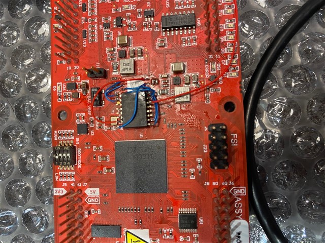
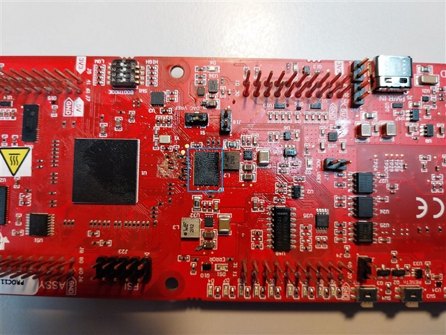
1. We are  trying to use MT25QL512ABB this flash. We put it on LP-AM263x and run qspi_flash_diag_am263x demo project and get json file as attachment.

[Cortex_R5_0] [QSPI Flash Diagnostic Test] Starting ...
[QSPI Flash Diagnostic Test] Flash Manufacturer ID : 0x20
[QSPI Flash Diagnostic Test] Flash Device ID       : 0xBA20
[QSPI Flash Diagnostic Test] Executing Flash Erase on first block...
[QSPI Flash Diagnostic Test] Done !!!
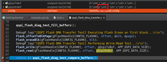
[QSPI Flash Diagnostic Test] Performing Write-Read Test...
[QSPI Flash Diagnostic Test] Write-Read Test Passed!
[QSPI Flash Diagnostic Test] SFDP Information : 
================================================
                      SFDP                      
================================================
SFDP Major Revision                       : 0x1
SFDP Minor Revision                       : 0x6
Number of Parameter Headers in this Table : 2

Types of Additional Parameter Tables in this flash
---------------------------------------------------
4 BYTE ADDRESSING MODE INSTRUCTIONS TABLE

{

	"flashSize": "67108864",
	"flashPageSize": "256",
	"flashManfId": "0x20",
	"flashDeviceId": "0xBA20",
	"flashBlockSize": "65536",
	"flashSectorSize": "4096",
	"cmdBlockErase3B": "0xD8",
	"cmdBlockErase4B": "0xDC",
	"cmdSectorErase3B": "0x20",
	"cmdSectorErase4B": "0x21",
	"protos": {
		"p111": {
			"isDtr": false,
			"cmdRd": "0x03",
			"cmdWr": "0x02",
			"modeClksCmd": 0,
			"modeClksRd": 0,
			"dummyClksCmd": 0,
			"dummyClksRd": 0,
			"enableType": "0",
			"enableSeq": "0x00",
			"dummyCfg": null,
			"protoCfg": null,
			"strDtrCfg": null,
		},
		"p112": {
			"isDtr": false,
			"cmdRd": "0x3C",
			"cmdWr": "0x02",
			"modeClksCmd": 0,
			"modeClksRd": 1,
			"dummyClksCmd": 0,
			"dummyClksRd": 7,
			"enableType": "0",
			"enableSeq": "0x00",
			"dummyCfg": null,
			"protoCfg": null,
			"strDtrCfg": null,
		},
		"p114": {
			"isDtr": false,
			"cmdRd": "0x6C",
			"cmdWr": "0x34",
			"modeClksCmd": 0,
			"modeClksRd": 1,
			"dummyClksCmd": 0,
			"dummyClksRd": 7,
			"enableType": "0",
			"enableSeq": "0x00",
			"dummyCfg": null,
			"protoCfg": null,
			"strDtrCfg": null,
		},
		"p118": null,
		"p444s": null,
		"p444d": null,
		"p888s": null,
		"p888d": null,
		"pCustom": null
	},
	"addrByteSupport": "1",
	"fourByteAddrEnSeq": "0x36",
	"resetType": "0x3D",
	"cmdWren": "0x06",
	"cmdRdsr": "0x05",
	"srWip": 0,
	"srWel": 0,
	"cmdChipErase": "0xC7",
	"flashDeviceBusyTimeout": 128000000,
	"flashPageProgTimeout": 120
}

All tests have passed!!

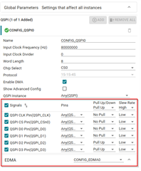
2. We have checked the following settings

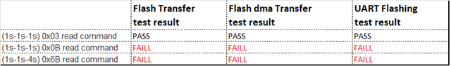
- Check for 1s-1s-1s mode (We use 1s mode), WEL have to set 1.  - done

- HW reliability  : Make sure Micron flash can pass boot qspi_flash_dms_transfer (32KB) & qspi_flash_transfer (256B) test - pass

- To increase your timeout value since SPI mode is much slower - done

3. Please find the final settings we configure.

/* FLASH Attrs */
/* FLASH Attrs - populated from SysConfig options */
Flash_Attrs gFlashAttrs_MT25QL512ABB =
{
    .flashName = "MT25QL512ABB",
    .deviceId = 0xBA20,
    .manufacturerId = 0x20,
    .flashSize = 67108864,
    .blockCount = 1024,
    .blockSize = 65536,
    .pageCount = 256,
    .pageSize = 256,
    .sectorCount = 16384,
    .sectorSize = 4096,
};

/* FLASH DevConfig */
/* FLASH DevConfig - populated from SysConfig options */
Flash_DevConfig gFlashDevCfg_MT25QL512ABB =
{
    .enable4BAddr = false,
    .addrByteSupport = 0x00,
    .fourByteAddrEnSeq = 0x00,
    .cmdWren = 0x06,
    .cmdRdsr = 0x05,
    .srWip = (1 << 0),
    .srWel = (1 << 1),
    .resetType = 0x1D,
    .eraseCfg = {
        .blockSize = 65536,
        .sectorSize = 4096,
        .cmdBlockErase3B = 0xD8,
        .cmdBlockErase4B = 0xD8,
        .cmdSectorErase3B = 0x20,
        .cmdSectorErase4B = 0x20,
        .cmdChipErase = 0xC7,
    },
    .idCfg = {
        .cmd = 0x9F, /* Constant */
        .numBytes = 3,
        .dummy4 = 0,
        .dummy8 = 0,
    },
    .protocolCfg = {
        .protocol = FLASH_CFG_PROTO_1S_1S_1S,
        .isDtr = FALSE, /* DTR not supported in this version of flash driver with QSPI */
        .cmdRd = 0x03,
        .cmdWr = 0x02,
        .modeClksCmd = 0,
        .modeClksRd = 0,
        .dummyClksCmd = 0,
        .dummyClksRd = 0,
        .enableType = 0xFF,
    },
    .flashWriteTimeout = 4000,
    .flashBusyTimeout = 128000000,
};

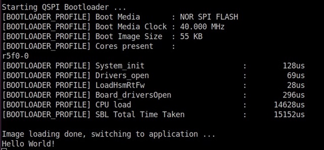
However, the issues we have encountered so far, we can use flash writer to write image into Micron flash, but we can't boot SBL.

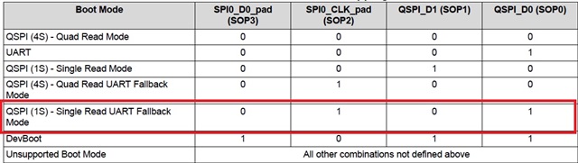
We set QSPI (1S) - Single Read UART Fallback Mode, but after restarting the power supply, SBL fails to start, so start from external host via UART interface.

  • Otherwise is AM263x ROM code is capable to support MT25QL512ABB flash?

  • Hi ,

    Did you happen to rebuilt the SBL on your end or you are trying to boot the sbl_null *.tiimage provided by MCU_PLUS_SDK out of the box ?

    If you have rebuilt the SBL on your end, I would suggest you to check the OpenSSL version on your host machine (where you built the SBL). Make sure the version should be OpenSSL 1.1.1l only.

    My suggestion would be to start with sbl_null image provided by MCU_PLUS_SDK out of box.

    Best Regards,
    Aakash

  • Dear Aakash:

    1.According your suggection we started to use the sbl_null example code to debug and list the message, please help us to check if there is any problem

    Cortex_R5_0: GEL Output: Loading Gel Files on R5F0 
    Cortex_R5_0: GEL Output: Gel files loading on R5F0 Complete
    Cortex_R5_0: GEL Output: ***OnTargetConnect() Launched***
    
    Cortex_R5_0: GEL Output: AM263x Initialization Scripts Launched. 
    Please Wait...
    
    
    Cortex_R5_0: GEL Output: AM263x_Cryst_Clock_Loss_Status() Launched
    Cortex_R5_0: GEL Output: Crystal Clock present 
    Cortex_R5_0: GEL Output: AM263x_SOP_Mode() Launched
    Cortex_R5_0: GEL Output: SOP MODE = 0x00000005    
    Cortex_R5_0: GEL Output: 
     QSPI - 1S Fallback UART boot mode
    Cortex_R5_0: GEL Output: AM263x_Read_Device_Type() Launched
    Cortex_R5_0: GEL Output: EFuse Device Type Value = 0x000000AA    
    Cortex_R5_0: GEL Output: AM263x_Check_supported_mode() Launched
    Cortex_R5_0: GEL Output: 
     efuse1=0x01000000  
    Cortex_R5_0: GEL Output: 
     The Device supports both LockStep & Dual Core mode 
    Cortex_R5_0: GEL Output: 
     mode = 0 
    Cortex_R5_0: GEL Output: MSS_CTRL Control Registers Unlocked
    Cortex_R5_0: GEL Output: MSS_TOP_RCM Control Registers Unlocked
    Cortex_R5_0: GEL Output: MSS_RCM Control Registers Unlocked
    Cortex_R5_0: GEL Output: MSS_IOMUX Control Registers Unlocked
    Cortex_R5_0: GEL Output: TOP_CTRL Control Registers Unlocked
    Cortex_R5_0: GEL Output: 
    
    ***R5FSS0 Reset for Lockstep ***
    Cortex_R5_0: GEL Output: 
    
    *** R5FSS1 Reset for Lockstep ***
    Cortex_R5_0: GEL Output: R5F ROM Eclipse
    Cortex_R5_0: GEL Output: R5FSS0_0 Released
    Cortex_R5_0: GEL Output: R5FSS0_1 Released
    Cortex_R5_0: GEL Output: R5FSS1_0 Released
    Cortex_R5_0: GEL Output: R5FSS1_1 Released
    Cortex_R5_0: GEL Output: 
    
     All R5F Cores Released for program load
    Cortex_R5_0: GEL Output: L2 Mem Init Complete
    Cortex_R5_0: GEL Output: MailBox Mem Init Complete
    Cortex_R5_0: GEL Output: *********** R5FSS0/1 Lockstep mode Configured********
    Cortex_R5_0: GEL Output: PER PLL Configuration Complete
    Cortex_R5_0: GEL Output: SYS_CLK DIVBY2 
    Cortex_R5_0: GEL Output: DPLL_CORE_HSDIV0_CLKOUT0 selected as CLK source for R5FSS & SYS CLKs 
    Cortex_R5_0: GEL Output: 
     CLK Programmed R5F=400MHz and SYS_CLK=200MHz 
    Cortex_R5_0: GEL Output: 
    
     *** Enabling Peripheral Clocks *** 
    Cortex_R5_0: GEL Output: Enabling RTI[0:3] Clocks 
    Cortex_R5_0: GEL Output: Enabling RTI_WDT[0:3] Clocks 
    Cortex_R5_0: GEL Output: Enabling UART[0:5]/LIN[0:5] Clocks 
    Cortex_R5_0: GEL Output: Enabling QSPI Clocks 
    Cortex_R5_0: GEL Output: Enabling I2C Clocks 
    Cortex_R5_0: GEL Output: Enabling TRACE Clocks 
    Cortex_R5_0: GEL Output: Enabling MCAN[0:3] Clocks 
    Cortex_R5_0: GEL Output: Enabling GPMC Clocks 
    Cortex_R5_0: GEL Output: Enabling ELM Clocks 
    Cortex_R5_0: GEL Output: Enabling MMCSD Clocks 
    Cortex_R5_0: GEL Output: Enabling MCSPI[0:4] Clocks 
    Cortex_R5_0: GEL Output: Enabling CONTROLSS Clocks 
    Cortex_R5_0: GEL Output: Enabling CPTS Clocks 
    Cortex_R5_0: GEL Output: Enabling RGMI[5,50,250] Clocks 
    Cortex_R5_0: GEL Output: Enabling XTAL_TEMPSENSE_32K Clocks 
    Cortex_R5_0: GEL Output: Enabling XTAL_MMC_32K Clocks 
    Cortex_R5_0: GEL Output: 
    
     ***All IP Clocks are Enabled*** 
    
    Cortex_R5_0: GEL Output: CPU reset (soft reset) has been issued through GEL.
    

    2.BTW For openssl version,
    - We have tried 1.1.1f, 1.1.1q for Linux, 1.1.1s for windows, but the problem of "SBL cannot boot" has not been solved,

    - Now  we are installing 1.1.1l on linux, but we have some problems and still keep ongoing to process it!!

    In addition, there is a problem, if it is because of the openssl version, but why we test the result of infineon S25FL128SA, "SBL boot is normal"

    Best regards,

    Wilson

  • Hi ,

    We have tried 1.1.1f, 1.1.1q for Linux, 1.1.1s for windows, but the problem of "SBL cannot boot" has not been solved,

    Instead of juggling around the openssl versions, I would suggest to send the sbl_null example *.tiimage via XMODEM in UART Boot Mode. If that works for you, then the SBL images are correctly functional.

    You already mentioned you tried to program the image via flash writer. Did you use the sbl_uart_uniflash or the sbl_jtag_uniflash for the same ?

    If yes, did you update the required flash related changes in the sysconfig for the above mentioned SBLs ?

    Best Regards,
    Aakash

  • Dear Aakash:

    1.I see that TI document mentions "Good signal integrity of this memory interface is critical for basic QSPI boot operations of the AM263x MCU" May I ask if we replace the Infineon flash on the LP-AM263x with the MT25QL512ABB flash as below picture , will it be the possible reason for "flash can not boot issue"?

    2.Here is the answer to your question

    - You already mentioned you tried to program the image via flash writer. Did you use the sbl_uart_uniflash or the sbl_jtag_uniflash for the same ?

    -> We use uart_uniflash_gui.py to program the image as below picture

    - If yes, did you update the required flash related changes in the sysconfig for the above mentioned SBLs ?

    -> Yes. please find the sysconfilg files as below

    a.sbl_uart_uniflash

    example_syscfg_sbl_uniflash.zip

    2.sbl_qspi

    example_syscfg_sbl_qspi.zip

    3.App image

    example_syscfg_app_image.zip

    Best regards,

    Wilson

  • Hi Wilson,

    I cannot deduce why isn't the SPI boot mode functional for you. Seems like a lot of your details are absolutely correct.

    Experiments Results
    Flash Diag (1s-1s-1s)

    PASS

    Flash Transfer (1s-1s-1s)

    PASS

    UART Flashing (1s-1s-1s)

    PASS

    ROM Boot (1s-1s-1s)

    FAIL

    Just to confirm that the boot mode on the LP you have set is QSPI (1s) which is 0101. Launchpad should be in 1010 i.e. something like this.

    Can you please try the same and confirm ? This is because, QSPI might work or might not work depending on the hardware settings but the SPI hardware is absolutely verified by you, I suggest you to start with SPI boot.

    Best Regards,
    Aakash

  • Dear Aakash :

    1.Let me confirm with you the following

    • Flash Diag (1s-1s-1s) PASS <-- YES
    • Flash Transfer (1s-1s-1s) PASS <-- YES
    • Flash dma Yransfer (1s-1s-1s) PASS <-- YES
    • UART Flashing (1s-1s-1s) PASS <--- YES
    • ROM Boot (1s-1s-1s) FAIL <-- YES

    2. We refer to the ROM Sequence(1s-1s-1s) in the TRM file and check as follows:
            • Command issued by ROM in this mode is 0x0B.
               -> We had confirmed that the specification of Miron flash supports it.
            • RBL looks for SBL image at address 0x0000_0000, in case of boot failures due to corrupted image
               -> May I ask if it is the corrupted sbl image that caused the Boot issues, or the replacement of the flash by HW r?

    Best regards,

    Wilson

  • Dear Aakash :

    Can you please try the same and confirm ?

    -> We have repeatedly confirmed that the BOOTMODE Pin(1s-1s-1s) is correct, just like your captured picture.

    Best regards,

    Wilson

  • Wilson, Aakash,

         Based support today, we tested two boards with the same code.  one board even can't pass qspi_flash_diag in 1s-1s-1s mode.

    The other board can use python scripts to load sbl_uart_uniflash and program sbl_null successfully. However, it still fail to boot up.

    I suggest you check your HW quality since we got two different results by using the same code. 

    Base on my understanding, if sbl_uart_uniflash can be executed, the SW development is OK. There should be no mistake in Flash driver setting.

    OpenSSL signature tool should be good.

    It's highly possibility fail in x.509 certification after ROM code load image to RAM i.e. the content load from FLASH to RAM is not correct.

    You can refer to Initialization section in TRM for more detail.

    Regards

    Andre

  • Hi  and ,

    Let's have a short call to debug the same. Please send an invite for the same today.

    Best Regards,
    Aakash

  • let's have a short discussion. Send you invitation by mail.

    Regards

    Andre

  • Hi ,

    As discussed, let me discuss internally and work on the next action items.

    Best Regards,
    Aakash

  • Hi AndreTseng,

    We have provided an application note to choose supported flashes - https://www.ti.com/lit/an/sprad50/sprad50.pdf

    We are working on ROM troubleshooting guidelines. We will provide the same shortly.

    Hope this helps.

    Best Regards,
    Aakash

  • Dear Aakash :

    According to TI's suggestion, we replaced MT25QL128ABA1EW9, because only 128Mb has pin-to-pin package,
    but the verification result is still the same

    Flash Diag (1s-1s-1s) PASS
    Flash Transfer (1s-1s-1s) PASS
    Flash dma Yransfer (1s-1s-1s) PASS
    UART Flashing (1s-1s-1s) PASS
    ROM Boot (1s-1s-1s) FAIL

    Do you have any other suggestions?

    Wilson

  • Aakash,

         Please provide a way to check ROM code issue today. And we did not get any confirmation about if ROM code support this Flash or not. Please advice how to overcome this problem.

    Regards

    Andre

  • Hi  and ,

    Apologies for the delay. We would need more logs from RBL to find out what went wrong here. That will be provided by EoD.

    Best Regards,
    Aakash

  • Dear Aakash :

    In order to avoid confusion, I compiled a table. The verification results from the table show that (1s-1s-1s) with 0x0B read command & (1s-1s-4s) with 0x6B read command all failed

    Wilson

  • Wilson,

          Did you add 8 dummy cycles when you use 0x0B fast read  command? It needs to modify low level driver lib before you compile flash diagram and Xfer test utilities. If you just modify syscfg in these application, it won’t work. Please check driver source code.

    Regards

    Andre

  • Hi Wilson Sun,

    The Datasheet mentions that the 0x3 is the valid read command for 1s-1s-1s and for fast read (0x0B) you should also set the dummy cycles as 8 or higher.

    For 1s-1s-4s i.e. 0x6B you must make sure that the dummy cycles is 10 or higher. Also make sure the QE bit is set.

    Best Regards,
    Aakash

  • Dear Aakash:

    It needs to modify low level driver lib before you compile flash diagram and Xfer test utilities.

    -> 

    1. We are trying to find a low level driver, but it si very urgent for us , can you tell us how to change it?
    2. Is the ROM code boot failure also related to this?

    Wilson

  • Dear Aakash:

    The Datasheet mentions that the 0x3 is the valid read command for 1s-1s-1s and for fast read (0x0B) you should also set the dummy cycles as 8 or higher.
    ->
    1. If we want to solve the problem that the ROM code cannot be booted, should we first confirm that the 0x0B (1s-1s-1s) or 0x6B (1s-1s-4s) read command can pass the verification of the dma transfer & flash transfer program?

    2. We have already set 8 dummy in syscfg, we will change it to low level driver according to your suggestion.

    Wilson

  • Hi ,

    My suggestion would be to start with 0x0B (1s-1s-1s) because with 0x3 CMD you have already confirmed that the your hardware lines are okay with 1-1-1. 

    If you just modify syscfg in these application, it won’t work. Please check driver source code

     - I didn't find anything wrong with the syscfg.QeBit is only required for 1-1-4 mode. The Enable Type is 2 in this case.

    Best Regards,
    Aakash

  • Dear Aakash:

    1. My suggestion would be to start with 0x0B (1s-1s-1s) 

    -> We use "dma transfer" to verify it ! it always fails and show below message.

    [Cortex_R5_0] [QSPI Flash DMA Transfer Test] Starting ...
    [QSPI Flash DMA Transfer Test] Executing Flash Erase on first block...
    [QSPI Flash DMA Transfer Test] Performing Write-Read Test...
    ERROR: qspi_flash_diag_test_compare_buffers:124: QSPI read data mismatch !!!
    Some tests have failed!!

    2.Although the specification of Micron flash conforms to AM263x_QSPI_Flash_Selection_Guide_sprad50, the actual verification fails. Does the TI MCU support Micron's NOR flash (MT25QL128ABA or MT25QL512ABB ) ?

    3.Please refer to our SFDP and sysconfig file for Micron MT25QL128ABA

    SFDP_and_sysconfig.zip

    Wilson

  • Dear Aakash:

    When using the 0x0B read command, it is found that when running the dma transfer program, one more ('0') will be read, as shown in the figure below, every 31 bytes behind the Array, there will be one more '0'

    Wilson

  • Hi ,

    What is the dummy cycles used ? Is it 8 ? Can you try with 7 ?

    Best Regards,
    Aakash

  • Dear Aakash:

    As you said, we changed the low level driver to let the transfer program pass the test, as follows

    Flash Diag (1s-1s-1s with 0x0B read cmd/dummy 8/qspi clock 40Mhaz) PASS
    Flash Transfer (1s-1s-1s with 0x0B read cmd/dummy 8/qspi clock 40Mhaz) PASS
    Flash dma Yransfer (1s-1s-1s with 0x0B read cmd/dummy 8/qspi clock 40Mhaz) PASS
    UART Flashing (1s-1s-1s with 0x0B read cmd/dummy 8/qspi clock 40Mhaz) PASS
    ROM Boot (1s-1s-1s)  FAIL

    Could you have any suggestion for next action ?

    Thanks!


    Wilson

  • Hi ,

    We are in discussion of debug for this. Would you migrate to 1-1-4 mode now ?

    Best Regards,
    Aakash

  • Dear Aakash:

    We are in discussion of debug for this. Would you migrate to 1-1-4 mode now ?

    -> I have tried to test dma transfer (1s-1s-4s with 0x6B read cmd/dummy 8/QE 2/qspi clcok 80Mhz) and the verification result is fails now.

    Wilson

  • Hi ,

    • Can you decrease the frequency to 40MHz and then test the same ?
    • Can you increase the dummy cycles to 10 ?
    • Can you share the exact read and write values in the buffer like this -

    When using the 0x0B read command, it is found that when running the dma transfer program, one more ('0') will be read, as shown in the figure below, every 31 bytes behind the Array, there will be one more '0'

    Best Regards,
    Aakash

  • Dear Aakash:

    Can you share the exact read and write values in the buffer

    -> I dump the memory as attached file.

    memory_dump.zip

    example_for_MT25QL128ABA_1s1s4s.zip

    Thanks!

    Wilson

  • Hi ,

    Thanks for sharing the information. We have analyzed this and there are 2 options -

    1. The dummy cycles are too high. Try reducing the dummy cycles to 3~4 and 1~2 and please share the dump.
    2. There might be some problem in some data lines apart from D0. We need to probe the lines and get more information on the same.

    Best Regards,
    Aakash

  • Dear Aakash

    1. The dummy cycles are too high. Try reducing the dummy cycles to 3~4 and 1~2 and please share the dump.

    -> Reduce the number of dummy, the read test will make more mistakes, please refer to the attached

    memory_dump_v2.zip

    2.BTW we use ccstudio 12.2.0 (06 Jan 2023) and SDK Version: 08.05.00.24 for development, it will this affect? Do I need to return the OLD version? which is stable version ?

    Best regards,

    Wilson

  • Hi ,

    -> Reduce the number of dummy, the read test will make more mistakes, please refer to the attached

    It seems like the dummy cycles set as 10 was perfect. We need to probe the hardware.

    2.BTW we use ccstudio 12.2.0 (06 Jan 2023) and SDK Version: 08.05.00.24 for development, it will this affect? Do I need to return the OLD version? which is stable version ?

    Latest versions of SDK as deemed to be more stable versions of SDK. Please stick to the same.

    Best Regards,
    Aakash

  • Dear Aakash

    1.It seems like the dummy cycles set as 10 was perfect. We need to probe the hardware.

    -> But the dma transfer of 1s-1s-1s with 0x0B read coammdn passed the verification. The hardware looks fine, why the ROM code still can’t BOOT ?

    2.How to prove sbl_qspi and prove that it is no problem? 

    Best regards,

    Wilson 

  • Hi ,

    -> But the dma transfer of 1s-1s-1s with 0x0B read coammdn passed the verification. The hardware looks fine, why the ROM code still can’t BOOT ?

    The 1s-1s-1s uses only 1 data line D0 for command as well as data where as 1-1-4 uses 1 data line for command but 4 data lines i.e. D0, D1, D2, D3 for sending the data. ROM booting is still in debug.

    Best Regards,
    Aakash

  • Dear Aakash:

    1.We only need 1s-1s-1s, so only use D0 line. If the quality of hardware D1, D2, D3 line is not good, will it affect the ROM code root?

    2.How to prove sbl_qspi and prove that it is no problem? 

    Best regards,

    Wilson

  • Hi ,

    We only need 1s-1s-1s, so only use D0 line. If the quality of hardware D1, D2, D3 line is not good, will it affect the ROM code root?

    In case of 1s-1s-1s, only D0 line will be required. ROM Code will not be affected with quality of hardware. According to your use case, you do not intend to use 1-1-4 at all ?

    2.How to prove sbl_qspi and prove that it is no problem? 

    I have a suggestion (just a hack) which will give you good confidence.

    1. For now you can program SBL, Application etc. via UNIFLASH which is working for you.
    2. Now put the device in UART Boot Mode, and send the sbl_qspi.tiimage via XMODEM (using Tera Term or xmodem utility of linux)

    This will boot your SBL_QSPI via RAM and the SBL_QSPI will boot the application via Flash. You can try this flow for now. Apologies for the inconvenience but we are working on the fix.

    Best Regards,
    Aakash

  • Dear Aakash:

    In case of 1s-1s-1s, only D0 line will be required. ROM Code will not be affected with quality of hardware. According to your use case, you do not intend to use 1-1-4 at all ?

    -> Yes , we do not use 1-1-4 at all.

    Best regards,

    Wilson

  • Hi Wilson Sun,

    Let me know if you try the method -

    I have a suggestion (just a hack) which will give you good confidence.

    1. For now you can program SBL, Application etc. via UNIFLASH which is working for you.
    2. Now put the device in UART Boot Mode, and send the sbl_qspi.tiimage via XMODEM (using Tera Term or xmodem utility of linux)

    This will boot your SBL_QSPI via RAM and the SBL_QSPI will boot the application via Flash. You can try this flow for now. Apologies for the inconvenience but we are working on the fix.

    Also can you share the updated schematic of this board and connection to AndreTseng ? 

    The flash lines that require pull up can be handled in MCU_PLUS_SDK but ROM does not do any pull up settings. Hence the external pull up should be done via user.

    Best Regards,
    Aakash

  • Dear Aakash

    1.Let me know if you try the method ,This will boot your SBL_QSPI via RAM and the SBL_QSPI will boot the application via Flash.

    -> Thanks for your suggestion  Please find the verification result as below

    2.Also can you share the updated schematic of this board and connection to AndreTseng ? 

    -> We are now doing verification on the TI EVM board, just replacing the Micron pin-to-pin flash MT25QL128ABA1EW9-0SIT, you mean the circuit diagram of the TI EVM is needed?

    3.ROM does not do any pull up settings. Hence the external pull up should be done via user.

    -> 

    1.We are now doing verification on the TI EVM board, why does the default S25FL128S flash not have boot problems?

    2.The 1s-1s-1s setting does not use D2, D3, why the ROM code cannot be booted as well?

    Best regards,

    Wilson

  • Hi ,

    Thanks for your suggestion  Please find the verification result as below

    This looks great.

    -> We are now doing verification on the TI EVM board, just replacing the Micron pin-to-pin flash MT25QL128ABA1EW9-0SIT, you mean the circuit diagram of the TI EVM is needed?

    Then we need to find the differences in the flash.

    2.The 1s-1s-1s setting does not use D2, D3, why the ROM code cannot be booted as well?

    That's correct, we need to evaluate the same with our hardware experts. Let me loop in the expert for the same. Due to Public Holiday in US, please expect delay in response.

    Best Regards,
    Aakash

  • Wilson,

         I think you need to double confirm with Micron, according this datasheet of MT25QL128ABA datasheet, DQ2/W# don't have internal pull ups. It can be float and need be be driven, This is different than Flash on EVM.   

    Regards

    Andre

  • Can you SET bootstrap configuration to b’0010 and try ? 

    Also connect to R5 code and share following memory dump

    4KB from 0x80000

    4KB from 0x70000000

    4KB from 0x60000000

    I am considering IO2/IO3 PUs are present.

    Thanks & Regards,

    Ajay


  • Ajay,

         Please confirm your request:

    1.  Can you SET bootstrap configuration to b’0010 and try ? 

    => do you mean try to boot in QSPI Single Read Mode and see if board can boot successfully?

    2. Also connect to R5 code and share following memory dump

    => in Debug mode??? 

    4KB from 0x80000

    4KB from 0x70000000

    4KB from 0x60000000

    I am considering IO2/IO3 PUs are present.

    Thanks & Regards,

    Regards

    Andre

  • Andre ,

    Please find my  comments for the respective queries.

    1. Yes , It is 1S-1S-1S mode , want to check , Data has any corruption due to which boot is failing , Ideally this mode should work.

    Device also suipports , FAST read for with ReadCommad 0x0B and Dummy Cycles 8

    2, Memory dump in Functional Single Read mode only

    Thanks & Regards,

    Ajay

  • 2, Memory dump in Functional Single Read mode only

    If SBL doesn't run, we can't put it wait in a while loop, how to connect R50_0 by JTAG in functional mode? 

    Regards

    Andre

  • Andre,

    R5_0 can't be connected only when HSM(M4)  doesn't un-halt R5 due to severe faults at HSM start up .

    Even if there are failures during sbl download , R5 can be connected.

    Its HSFS device right?

    Thanks & Regards,

    Ajay

  • Hi all,

       Issue closed by add 10K ohm external pull-up resistors on DQ2/WP# and DQ3/Hold# pin. 

    According to Micro Flash datasheet, these two pins do not have internal pull-up, external pull-up are mandatory.

    We strongly suggest qspi_dma_transfer test demo project use identical setting with RBL no matter 1s-1s-1s mode or 1s-1s-4s mode. 

    In this case, QSPI is set to mode3@40Mhz. DQ2,DQ3 should be set to no pull.  Flash use 0x0B command with 8 dummy read clock cycles. 

    We can find issue more efficiently.

    Regards

    Andre