Hello,
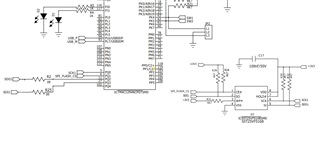
I'm trying to use SPI communication between TM4C1294NCPDT and SST25VF016B. Slave device MISO (SDI1)(SPI Flash SST25VF016B )is not responding .
Please refer the enclosed code , circuit and help to resolve the issue.
Thank you.
.
#include <stdbool.h>
#include <stdint.h>
#include "inc/hw_memmap.h"
#include "inc/hw_ints.h"
#include "driverlib/debug.h"
#include "driverlib/gpio.h"
#include "driverlib/interrupt.h"
#include "driverlib/pin_map.h"
#include "driverlib/rom.h"
#include "driverlib/rom_map.h"
#include "driverlib/ssi.h"
#include "driverlib/sysctl.h"
#include "driverlib/uart.h"
#include "utils/uartstdio.h"
#include "inc/hw_ssi.h"
#include "inc/hw_types.h"

//*****************************************************************************
//
//! \addtogroup example_list
//! <h1>SSI Master-to-Slave Transfer (spi_master_slave_xfer)</h1>
//!
//! This example demonstrates how to configure SSI0 as a SSI Master and SSI1
//! as a SSI slave.  The master will send four characters on the master to the
//! slave using the legacy mode.  In legacy mode, one bit is sent on each
//! SSI Clock pulse.  Once the SSI slave receives the four characters in the
//! receive FIFO it will generate an interrupt.
//!
//! This example uses the following peripherals and I/O signals.  You must
//! review these and change as needed for your own board:
//! - SSI0 peripheral
//! - GPIO Port A peripheral (for SSI0 pins)
//! - SSI0Clk    - PA2
//! - SSI0Fss    - PA3
//! - SSI0TX     - PA4
//! - SSI0RX     - PA5
//!
//! - SSI1 peripheral
//! - GPIO Port B & E peripheral (for SSI1 pins)
//! - SSI1Clk    - PB5
//! - SSI1Fss    - PB4
//! - SSI1TX     - PE4
//! - SSI1RX     - PE5
//!
//! This example requires board level connection between SSI0 and SSI1.
//!
//! UART0, connected to the Virtual Serial Port and running at 115,200, 8-N-1,
//! is used to display messages from this application.
//
//*****************************************************************************

//****************************************************************************
//
// The variable g_ui32SysClock contains the system clock frequency in Hz.
//
//****************************************************************************

#define SCK1  GPIO_PIN_0
#define CS    GPIO_PIN_1
#define SDO0  GPIO_PIN_2
#define SDI0  GPIO_PIN_3

uint32_t g_ui32SysClock;
static uint8_t SPI1_Initialized = 0;
//==============================================================================
// Pin Configurations
//==============================================================================
// Initialize chip select as Output
//#define INIT_CS()       ((MAP_SysCtlPeripheralEnable(SYSCTL_PERIPH_GPIOQ))\
//                          (MAP_SysCtlPeripheralEnable(SYSCTL_PERIPH_SSI3))\
//                          (MAP_GPIOPinTypeGPIOOutput(GPIO_PORTQ_BASE, GPIO_PIN_1)))


#define SDSPICSAssert()      (MAP_GPIOPinWrite(GPIO_PORTQ_BASE, GPIO_PIN_1,0))  //(LATBCLR = (unsigned int)(BIT_15))
#define SDSPICSDeAssert()    (MAP_GPIOPinWrite(GPIO_PORTQ_BASE, GPIO_PIN_1,2))  //(LATBSET = (unsigned int)(BIT_15))

#define SST25_WRITE_BYTE(X)  (SPI1_WriteByte((X)))
#define SST25_READ_BYTE()    (SPI1_ReadByte())


#define SST25_WRITE_BYTE(X)      (MAP_SSIDataPut(SSI3_BASE,X))
#define SST25_READ_BYTE(X)       (X=MAP_SSIDataGetNonBlocking(SSI3_BASE,X))//SPI1_ReadByte()

void SPI_Flash_ResetWriteProtection(void);
uint8_t SPI_Flash_WriteBusy(void);
void SPI1_Init_HighSpeed(void);
void SPI1_DeInit(void);
uint32_t glbdatarx[20]={0};
extern void SPIFlashInit(uint32_t ui32Base, uint32_t ui32Clock, uint32_t ui32BitRate);
/************************************************************************
* SST25 Commands
************************************************************************/
#define SST25_CMD_WRSR  (unsigned)0x01  // Write Status Register
#define SST25_CMD_WRITE (unsigned)0x02
#define SST25_CMD_READ  (unsigned)0x03
#define SST25_CMD_RDSR  (unsigned)0x05  // Read Status Register
#define SST25_CMD_WREN  (unsigned)0x06
#define SST25_CMD_EWSR  (unsigned)0x50
#define SST25_CMD_ERASE (unsigned)0x60

//*****************************************************************************
//
// Global flag to indicate data has been received.
//
//*****************************************************************************
volatile uint32_t g_breceiveFlag = 0;

//*****************************************************************************
//
// Number of bytes to send and receive.
//
//*****************************************************************************
#define NUM_SSI_DATA            4

//////////////////////
void SPI_Flash_Init(void)
{
//    uint32_t ui32_TReset;
//
//    ui32_TReset=MAP_SysCtlClockGet()*3*.0000002; // 200 ns delay

  //  INIT_CS();

    MAP_SysCtlPeripheralEnable(SYSCTL_PERIPH_GPIOQ);
    MAP_SysCtlPeripheralEnable(SYSCTL_PERIPH_SSI3);
    MAP_GPIOPinTypeGPIOOutput(GPIO_PORTQ_BASE, GPIO_PIN_1);


//    SDSPICSAssert();
//    MAP_SysCtlDelay(ui32_TReset); // hold L
//    SDSPICSDeAssert();

    SPI1_Init_HighSpeed();

    SPI_Flash_ResetWriteProtection();

}

/////////////////////////

void SPI1_Init_HighSpeed(void)
{
    if(SPI1_Initialized)
       SPI1_DeInit();
   {


        MAP_GPIOPinConfigure(GPIO_PQ0_SSI3CLK);
        MAP_GPIOPinConfigure(GPIO_PQ1_SSI3FSS);
        MAP_GPIOPinConfigure(GPIO_PQ2_SSI3XDAT0); //tx
        MAP_GPIOPinConfigure(GPIO_PQ3_SSI3XDAT1); //rx


        MAP_SSIConfigSetExpClk( SSI3_BASE,  MAP_SysCtlClockGet(), SSI_FRF_MOTO_MODE_0,
                                    SSI_MODE_MASTER,
                                    (100000),
                                        8);
       SSIAdvModeSet(SSI3_BASE, SSI_ADV_MODE_READ_WRITE);//SSI_ADV_MODE_QUAD_WRITE);//SSI_ADV_MODE_READ_WRITE);//SSI_ADV_MODE_QUAD_WRITE);

      // MAP_SSIAdvFrameHoldEnable(SSI3_BASE);

       MAP_GPIOPinTypeSSI(GPIO_PORTQ_BASE,  GPIO_PIN_0 |GPIO_PIN_2 | GPIO_PIN_3 );

        MAP_SysCtlPeripheralEnable(SYSCTL_PERIPH_SSI3);

        MAP_SSIEnable(SSI3_BASE);

        SPI1_Initialized = 1;
   }
}
//////////
void SPI1_DeInit(void)
{
    MAP_SSIDisable(SSI3_BASE);//SpiChnClose(SPI_CHANNEL1);
    SPI1_Initialized = 0;
}
/////////////////////

void SPI_Flash_ResetWriteProtection(void)
{
        uint32_t ui32_TReset;

        ui32_TReset=MAP_SysCtlClockGet()*3*.0000002; // 200 ns delay

    SDSPICSAssert();

//    MAP_SSIDataPut(SSI3_BASE, (SST25_CMD_EWSR));
    MAP_SSIDataPutNonBlocking(SSI3_BASE, (SST25_CMD_EWSR));
    SDSPICSDeAssert();

    // Delay for next I/O
    MAP_SysCtlDelay(ui32_TReset); // hold L
  //  MAP_SSIDataPut(SSI3_BASE, (0));

    MAP_SSIDataPutNonBlocking(SSI3_BASE, (0));
    SDSPICSAssert();

    //MAP_SSIDataPut(SSI3_BASE, (SST25_CMD_WRSR));
    //MAP_SSIDataPut(SSI3_BASE, (0));

    MAP_SSIDataPutNonBlocking(SSI3_BASE, (SST25_CMD_WRSR));
    MAP_SSIDataPutNonBlocking(SSI3_BASE, (0));
    SDSPICSDeAssert();

  //  while (MAP_SSIBusy(SSI3_BASE));
    while(SPI_Flash_WriteBusy());
}

//////////////////////

/************************************************************************
* Function: void SST25ReadArray(DWORD address, uint8_t* pData, nCount)
*
* Overview: this function reads data into buffer specified
*
* Input: flash memory address, pointer to the data buffer, data number
*
************************************************************************/
void SPI_Flash_RawRead(uint32_t address, uint32_t *pData, uint32_t nCount)
{

    uint32_t temp=0xff,itr;
    union
    {
        uint32_t addr;
        char addrbyt[4];
    }un;
    un.addr=0;
    un.addr=address;

    SPI1_Init_HighSpeed();

    SDSPICSAssert();


 //  while((HWREG(SSI3_BASE + SSI_O_SR) & SSI_SR_RNE) )
    {

        MAP_SSIDataPut(SSI3_BASE, SST25_CMD_READ);
        MAP_SSIDataPut(SSI3_BASE, un.addrbyt[2]);
        MAP_SSIDataPut(SSI3_BASE, un.addrbyt[1]);
        MAP_SSIDataPut(SSI3_BASE, un.addrbyt[0]);

       //MAP_SSIDataGet(SSI3_BASE, &temp);  //dummy write

        //MAP_SSIDataPutNonBlocking(SSI3_BASE, SST25_CMD_READ);
        //MAP_SSIDataPutNonBlocking(SSI3_BASE, un.addrbyt[2]);
        //MAP_SSIDataPutNonBlocking(SSI3_BASE, un.addrbyt[1]);
        //MAP_SSIDataPutNonBlocking(SSI3_BASE, un.addrbyt[0]);

        //MAP_SSIDataGet(SSI3_BASE, &temp);  //dummy write

        //SSIAdvModeSet(SSI3_BASE, SSI_ADV_MODE_QUAD_READ);//SSI_ADV_MODE_QUAD_WRITE);

        while(nCount--)
        {

            *pData++= MAP_SSIDataGetNonBlocking(SSI3_BASE,pData);//SST25_READ_BYTE();
        }

      SDSPICSDeAssert();

    }

  //  SDSPICSDeAssert();
}
/************************************************************************
* Function: SST25WriteEnable()
*
* Overview: this function allows write/erase SST25. Must be called
* before every write/erase command.
*
* Input: none
*
* Output: none
*
************************************************************************/
void SPI_Flash_WriteEnable(void)
{
    SDSPICSAssert();

  // MAP_SSIDataPut(SSI3_BASE, SST25_CMD_WREN);
    MAP_SSIDataPutNonBlocking(SSI3_BASE, SST25_CMD_WREN);
    SDSPICSDeAssert();
}

/////////////
/************************************************************************
* Function: uint8_t SST25IsWriteBusy(void)
*
* Overview: this function reads status register and chek BUSY bit for write operation
*
* Input: none
*
* Output: non zero if busy
*
************************************************************************/
uint8_t SPI_Flash_WriteBusy(void)
{
    uint32_t Status;

    SDSPICSAssert();

    //MAP_SSIDataPut(SSI3_BASE, SST25_CMD_RDSR);
    //MAP_SSIDataGet(SSI3_BASE, &Status);

    MAP_SSIDataPutNonBlocking(SSI3_BASE, SST25_CMD_RDSR);
    Status = MAP_SSIDataGetNonBlocking(SSI3_BASE, &Status);

    SDSPICSDeAssert();

    return (Status & 0x01);
}

////////////////////////
void SPI_Flash_RawErase(void)
{
    SPI1_Init_HighSpeed();

    SPI_Flash_WriteEnable();

    SDSPICSAssert();

  //  MAP_SSIDataPut(SSI3_BASE, SST25_CMD_ERASE);
    MAP_SSIDataPutNonBlocking(SSI3_BASE, SST25_CMD_ERASE);
    SDSPICSDeAssert();

    // Wait for write end
    while(SPI_Flash_WriteBusy());
}

//////////
/************************************************************************
* Function: void SST25WriteByte(BYTE data, DWORD address)
*
* Overview: this function writes a byte to the address specified
*
* Input: data to be written and address
*
* Output: none
*
************************************************************************/
void SPI_Flash_WriteByte(uint8_t data, uint32_t address)
{
   uint8_t temp=0xff;
    union
    {
        uint32_t addr;
        uint8_t addrbyt[4];
    }un;
    address=25;
    un.addr=address;


    SPI_Flash_WriteEnable();

    SDSPICSAssert();

  //  MAP_SSIDataPut(SSI3_BASE, temp);  //dummy write


    MAP_SSIDataPut(SSI3_BASE, SST25_CMD_WRITE);

    MAP_SSIDataPut(SSI3_BASE, un.addrbyt[2]);
    MAP_SSIDataPut(SSI3_BASE, un.addrbyt[1]);
    MAP_SSIDataPut(SSI3_BASE, un.addrbyt[0]);

//    data = SPI1_ReadByte();
 //   SST25_WRITE_BYTE(data); ///SPI1_WriteByte(data);
    MAP_SSIDataPut(SSI3_BASE,data);

//    MAP_SSIDataPutNonBlocking(SSI3_BASE, SST25_CMD_WRITE);
//    MAP_SSIDataPutNonBlocking(SSI3_BASE, un.addrbyt[2]);
//    MAP_SSIDataPutNonBlocking(SSI3_BASE, un.addrbyt[1]);
//    MAP_SSIDataPutNonBlocking(SSI3_BASE, un.addrbyt[0]);
//    temp = SPI1_ReadByte();
//    SPI1_WriteByte(data);

//    HWREG(SSI3_BASE + SSI_O_DR)  = SST25_CMD_WRITE;
//    HWREG(SSI3_BASE + SSI_O_DR)  = un.addrbyt[0];
//    HWREG(SSI3_BASE + SSI_O_DR)  = un.addrbyt[1];
//    HWREG(SSI3_BASE + SSI_O_DR)  = un.addrbyt[2];
//    temp=HWREG(SSI3_BASE + SSI_O_DR);
//    HWREG(SSI3_BASE + SSI_O_DR)  = data;


    SDSPICSDeAssert();
    while(SPI_Flash_WriteBusy());

}
///////////////////////////

void SPI1_WriteByte(uint8_t Byte)
{
    uint32_t Data[2]={0};
    if(SPI1_Initialized)
    {

        //SpiChnPutC( SPI_CHANNEL1, (Byte))
        //MAP_SSIDataPut(SSI3_BASE,Byte);

        MAP_SSIDataPutNonBlocking(SSI3_BASE, (Byte));
        while((HWREG(SSI3_BASE + SSI_O_SR) & SSI_SR_RFF));// SSI_SR_RNE))

        MAP_SSIDataGetNonBlocking(SSI3_BASE, Data);
        //MAP_SSIDataGet(SSI3_BASE, Data);

        // while((HWREG(SSI3_BASE + SSI_O_DR) & SSI_SR_TNF))// && (1 & SSI_TXFF))
        //{
        // while((HWREG(SSI3_BASE + SSI_O_SR) & SSI_SR_TFE))
        //{
        //HWREG(SSI3_BASE + SSI_O_DR) =Byte;
        //while (MAP_SSIBusy(SSI3_BASE)); /// finish operation
        //Wait for byte to be sent
        //while(SPI1_RxBufferEmpty);
        //Discard Junk read
        //SpiChnGetC( SPI_CHANNEL1 );
        //MAP_SSIDataPut(SSI3_BASE,Data);
        //break;
        //}
    }

}
//////////
/************************************************************************
* Function: BYTE SST25WriteArray(DWORD address, BYTE* pData, nCount)
*
* Overview: this function writes a data array at the address specified
*
* Input: flash memory address, pointer to the data array, data number
*
* Output: return 1 if the operation was successfull
*
************************************************************************/
void SPI_Flash_RawWrite(uint32_t address, uint32_t *pData, uint32_t nCount)
{
    uint32_t   addr;
    uint8_t    *pD;
    uint32_t    counter;

    addr = address;
    pD = pData;
  //  while((HWREG(SSI3_BASE + SSI_O_SR) & SSI_SR_TNF))
    {

       SPI1_Init_HighSpeed();
      //  SDSPICSAssert();
        // WRITE
        for(counter = 0; counter < nCount; counter++)
        {
            SPI_Flash_WriteByte(*pD++, addr++);
        }
      //  SDSPICSDeAssert();
    }
}
/////////////
void PowerUpDelay(void)
{
    long int pwt=0;
    //INIT_CS();
    //SDSPICSAssert();

    for(pwt=0;pwt<500000;pwt++)  //~50ms delay (500000)
    {
        ;
    }

    //SDSPICSDeAssert();
}
//////////////////
uint8_t SPI1_ReadByte(void)
{
   uint32_t data=0;

   if(SPI1_Initialized)
    {
        // Write dummy to clock in data
      //  SpiChnPutC( SPI_CHANNEL1, (Dummy));

        //MAP_SSIDataPut(SSI3_BASE, 0xFF);
        MAP_SSIDataPutNonBlocking(SSI3_BASE, 0xFF);
        while((HWREG(SSI3_BASE + SSI_O_SR) & SSI_SR_RFF));// SSI_SR_RNE))

         //while(SPI1_RxBufferEmpty);

        // Return read byte
         MAP_SSIDataGetNonBlocking (SSI3_BASE,&data);

      //  MAP_SSIDataGet(SSI3_BASE,&data);
        return data;//SpiChnGetC( SPI_CHANNEL1 );

    }
    else
    {
    return 0;
    }
}

7

int main(void)
 {
    uint32_t pui32DataTx[NUM_SSI_DATA];
    uint32_t pui32DataTx1[NUM_SSI_DATA];
    uint32_t pui32DataRx[NUM_SSI_DATA];
    uint32_t ui32Index,ui32Reset1;
    uint32_t dely=0;

    PowerUpDelay();
    g_ui32SysClock = MAP_SysCtlClockFreqSet((SYSCTL_XTAL_25MHZ |
                                             SYSCTL_OSC_MAIN |
                                             SYSCTL_USE_PLL |
                                             SYSCTL_CFG_VCO_240), 120000000);

    pui32DataTx[0]=5; pui32DataTx[1]=6;
    SPI_Flash_Init();

    while (1)
    {


       SPI_Flash_RawWrite(25,pui32DataTx,1);

    }

}