Other Parts Discussed in Thread: UNIFLASH, SYSCONFIG
Hi expert,
I have question about Flash driver setting on AM2434 GP EVM.
1. I run ospi_flash_diag demo project to get SFDP data from default FLASH S28HS512T. Then I create json file for S28HS512T
[MAIN_Cortex_R5_0_0] [OSPI Flash Diagnostic Test] Starting ...
[OSPI Flash Diagnostic Test] Flash Manufacturer ID : 0x34
[OSPI Flash Diagnostic Test] Flash Device ID : 0x5B1A
[OSPI Flash Diagnostic Test] Executing Flash Erase on first block...
[OSPI Flash Diagnostic Test] Done !!!
[OSPI Flash Diagnostic Test] Performing Write-Read Test...
[OSPI Flash Diagnostic Test] Write-Read Test Passed!
[QSPI Flash Diagnostic Test] SFDP Information :
================================================
SFDP
================================================
SFDP Major Revision : 0x1
SFDP Minor Revision : 0x8
Number of Parameter Headers in this Table : 6
Types of Additional Parameter Tables in this flash
---------------------------------------------------
4 BYTE ADDRESSING MODE INSTRUCTIONS TABLE
NOR SPI PROFILE TABLE
STATUS CONTROL AND CONFIGURATION REGISTER MAP TABLE
OCTAL DDR MODE COMMAND SEQUENCE TABLE
SECTOR MAP TABLE
Parsing of OCTAL DDR MODE COMMAND SEQUENCE TABLE table not yet supported.
JSON Data for the flash :
{
"flashSize": 67108864,
"flashPageSize": 256,
"flashManfId": "0x34",
"flashDeviceId": "0x5B1A",
"flashBlockSize": 262144,
"flashSectorSize": 4096,
"cmdBlockErase3B": "0xDC",
"cmdBlockErase4B": "0xDC",
"cmdSectorErase3B": "0x21",
"cmdSectorErase4B": "0x21",
"protos": {
"p111": {
"isDtr": false,
"cmdRd": "0x03",
"cmdWr": "0x02",
"modeClksCmd": 0,
"modeClksRd": 0,
"dummyClksCmd": 0,
"dummyClksRd": 0,
"enableType": "0",
"enableSeq": "0x00",
"dummyCfg": null,
"protoCfg": null,
"strDtrCfg": null
},
"p112": null,
"p114": null,
"p118": null,
"p444s": null,
"p444d": null,
"p888s": null,
"p888d": {
"isDtr": true,
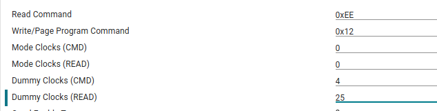
"cmdRd": "0xEE",
"cmdWr": "0x12",
"modeClksCmd": 0,
"modeClksRd": 0,
"dummyClksCmd": 4,
"dummyClksRd": 24,
"enableType": "0",
"enableSeq": "0x00",
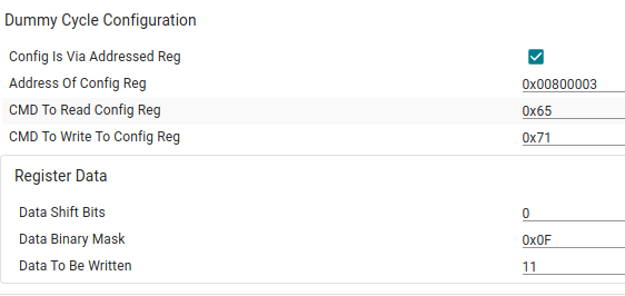
"dummyCfg": {
"isAddrReg": true,
"cmdRegRd":"0x65",
"cmdRegWr":"0x71",
"cfgReg":"0x00800003",
"shift":0,
"mask":"0x03",
"bitP":11
},
"protoCfg": {
"isAddrReg": true,
"cmdRegRd": "0x65",
"cmdRegWr": "0x71",
"cfgReg": "0x00800006",
"shift": 0,
"mask": "0x00",
"bitP": 0
},
"strDtrCfg": {
"isAddrReg": true,
"cmdRegRd": "0x65",
"cmdRegWr": "0x71",
"cfgReg": "0x00800006",
"shift": 1,
"mask": "0x00",
"bitP": 1
}
},
"pCustom": {
"fxn": null
}
},
"addrByteSupport": "1",
"fourByteAddrEnSeq": "0xA0",
"cmdExtType": "REPEAT",
"resetType": "0x10",
"deviceBusyType": "1",
"cmdWren": "0x06",
"cmdRdsr": "0x05",
"srWip": 0,
"srWel": 1,
"cmdChipErase": "0xC7",
"rdIdSettings": {
"cmd": "0x9F",
"numBytes": 5,
"dummy4": 0,
"dummy8": 0
},
"xspiWipRdCmd": "0x65",
"xspiWipReg": "0x00800000",
"xspiWipBit": 0,
"flashDeviceBusyTimeout": 256000000,
"flashPageProgTimeout": 512
}
All tests have passed!!
{

	"flashSize": 67108864,
	"flashPageSize": 256,
	"flashManfId": "0x34",
	"flashDeviceId": "0x5B1A",
	"flashBlockSize": 262144,
	"flashSectorSize": 4096,
	"cmdBlockErase3B": "0xDC",
	"cmdBlockErase4B": "0xDC",
	"cmdSectorErase3B": "0x21",
	"cmdSectorErase4B": "0x21",
	"protos": {
		"p111": {
			"isDtr": false,
			"cmdRd": "0x03",
			"cmdWr": "0x02",
			"modeClksCmd": 0,
			"modeClksRd": 0,
			"dummyClksCmd": 0,
			"dummyClksRd": 0,
			"enableType": "0",
			"enableSeq": "0x00",
			"dummyCfg": null,
			"protoCfg": null,
			"strDtrCfg": null
		},
		"p112": null,
		"p114": null,
		"p118": null,
		"p444s": null,
		"p444d": null,
		"p888s": null,
		"p888d": {
			"isDtr": true,
			"cmdRd": "0xEE",
			"cmdWr": "0x12",
			"modeClksCmd": 0,
			"modeClksRd": 0,
			"dummyClksCmd": 4,
			"dummyClksRd": 24,
			"enableType": "0",
			"enableSeq": "0x00",
			"dummyCfg": {
				"isAddrReg": true,
				"cmdRegRd":"0x65",
				"cmdRegWr":"0x71",
				"cfgReg":"0x00800003",
				"shift":0,
				"mask":"0x03",
				"bitP":11
			},
			"protoCfg": {
				"isAddrReg": true,
				"cmdRegRd": "0x65",
				"cmdRegWr": "0x71",
				"cfgReg": "0x00800006",
				"shift": 0,
				"mask": "0x00",
				"bitP": 0
			},
			"strDtrCfg": {
				"isAddrReg": true,
				"cmdRegRd": "0x65",
				"cmdRegWr": "0x71",
				"cfgReg": "0x00800006",
				"shift": 1,
				"mask": "0x00",
				"bitP": 1
			}
		},
		"pCustom": {
			"fxn": null
		}
	},
	"addrByteSupport": "1",
	"fourByteAddrEnSeq": "0xA0",
	"cmdExtType": "REPEAT",
	"resetType": "0x10",
	"deviceBusyType": "1",
	"cmdWren": "0x06",
	"cmdRdsr": "0x05",
	"srWip":  0,
	"srWel":  1,
	"cmdChipErase": "0xC7",
	"rdIdSettings": {
		"cmd": "0x9F",
		"numBytes": 5,
		"dummy4": 0,
		"dummy8": 0
	},
	"xspiWipRdCmd": "0x65",
	"xspiWipReg": "0x00800000",
	"xspiWipBit": 0,
	"flashDeviceBusyTimeout": 256000000,
	"flashPageProgTimeout": 512
}
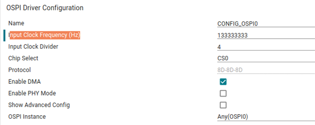
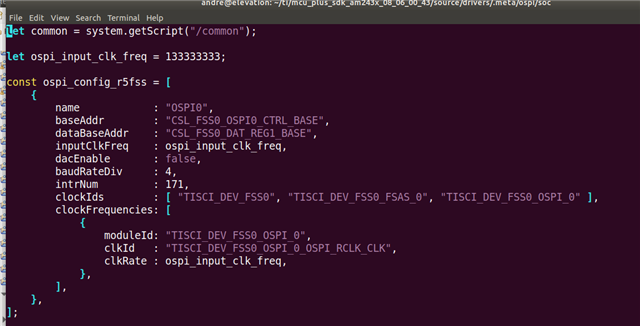
2. in sbl_uart_uniflash project, I create new customized configuration as
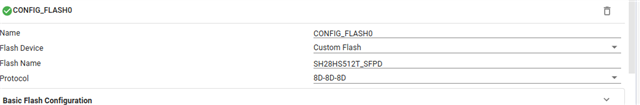
Load json file I got before. ( I use syscfg-tool 1.16 instead of default 1.14 since 1.4 has issue)
3. recompile it and use it as new flash writer. to program default sbl_null image.
However, the new sbl_uart_uniflash image doesn't work.

4. I compare the difference between default flash driver setting and load from json file. I find several setting are different.
I highlight here:

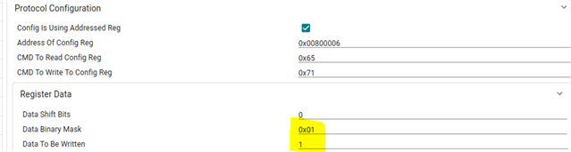
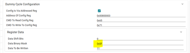
The dummy cycles setting, protocol enable configuration setting and register bit/bit mask are different then default.
4. I change back default setting and recompile it again, then every thing fine.
Question here.
1. Why default setting is deferent than result got from SFPD table? Which one match the FLASH datasheet description?
2. Automatically syscfg generated from "LOAD SFPD" json file doesn't work?
Regards
Andre