Part Number: MCU-PLUS-SDK-AM243X
Other Parts Discussed in Thread: UNIFLASH
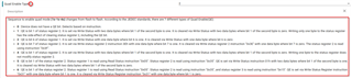
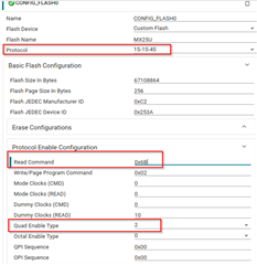
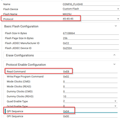
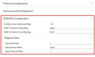
- I am facing issues while migrating the flash driver for custom flash.
- The flash does not work out of the box with the steps mentioned.
- How to debug the issues and I am new to the external flash environment ?
- Why is my UART Uniflash not working on my board ? Why is my JTAG Uniflash not working on my board ?