Because of the holidays, TI E2E™ design support forum responses will be delayed from Dec. 25 through Jan. 2. Thank you for your patience.

This thread has been locked.

If you have a related question, please click the "Ask a related question" button in the top right corner. The newly created question will be automatically linked to this question.

[FAQ] RM48L952: How to perform 8 Byte transfer in SCI Multi-buffered Mode using DMA

Part Number: RM48L952

When i was writing multi-buffered SCI using DMA in SCI2 Driver. However, my code was able to transmit up to 4 bytes, but when I tried to transmit 8 bytes, the RM48L952 stopped working. Even if I check the datasheet, it seems that there is buffer space and 8 Byte transmission is possible, but it does not work properly.

  • Hi,

    5226.Hercules SCI Mib with DMA spna213.pdf

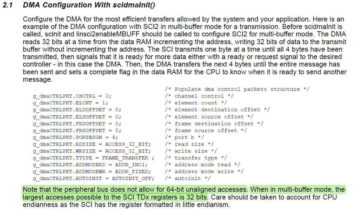
    If you verify the above app note "Hercules SCI with DMA", there you can see the below highlighted statement.

    Here they clearly mentioned that SCI_TDx registers will only support 32-bit access and it wont support 64bit access.

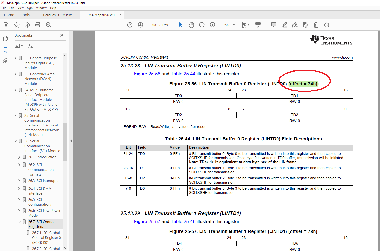
    which is because if you verify the starting offset address of these registers, it is 74h

    And the 74h (decimal 116) is not multiples of 8, so if we perform 8-byte access to these registers it leads to unaligned access and creates bus error. So, we have to use only 32-bit access for these registers because these registers addresses are multiples of 4, so use DMA with 32bit writes.

  • I can suggest you one way to utilize entire 8byte buffer of this SCI, that is by using 2 DMA channels. 

    The method i am suggesting is as below.

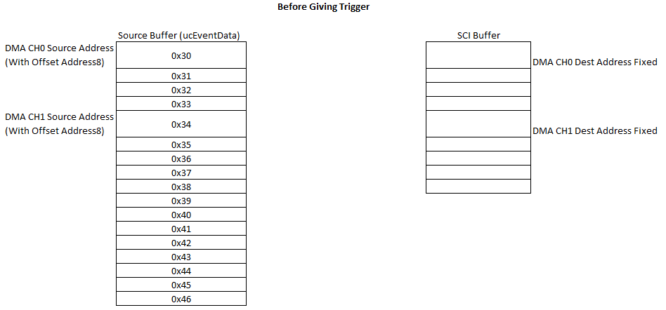
    Configure Two DMA channels with each 32 bit tranfer(i.e. 4 byte), The DMA source Read address should be offset of 8 byte (that means the address should increment by 8 after every frame transfer) and destination address should be fixed.

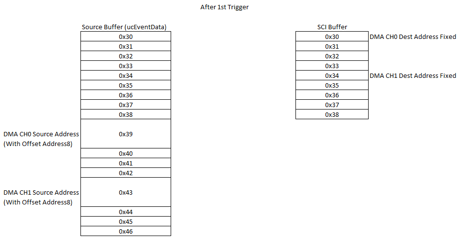
    If we do this after first trigger, it looks like below.

    After first frame trigger, the DMA CH0 writes the first 4 bytes from 0x30 to 0x33 to the first 4 addresses of SCI destination buffer and similarly DMA CH1 writes the second 4 bytes from 0x34 to 0x37 to the next 4 addresses of SCI destination buffer.

    After DMA CH0 finishes its writing, its source address will be increment by 8 as we configure this DMA channel with source offset of 8 and it will point to the 0x39 next time and similarly DMA CH1 source address also incremented by 4 and it will point to the 0x43 before second frame trigger.

    And this operation will continue. I am attaching the code for this method please verify and use it. 

    Note: I tested my code on RM46 you can just copy the main.c and paste it into your code and test it.

    1346.RM46_SCI_DMA.zip

    --

    Thanks,

    Jagadish.