This thread has been locked.

If you have a related question, please click the "Ask a related question" button in the top right corner. The newly created question will be automatically linked to this question.

TMS570LC4357: Write and read back operation on DMA Control Packet RAM

Part Number: TMS570LC4357

Hello,

In my project, I'm using 3 DMA channels assigned to 3 UART TX channels. The rest of the DMA channels should be unused. I have a requirement to ensure register writes and I'm doing it following way:

void WriteAndRead(volatile uint32_t* const pReg, const uint32_t value)
{
    *pReg = ((uint32_t)value);
    volatile uint32_t actualValue = *pReg;

    if ((actualValue & value) != value)
    {
        ErrorRaise(value, actualValue, *pReg, pReg)
    }
}

With the above code, I'm able to capture errors with really rare occurrence rates and with for example calling parameters ((uint32_t*)0xfff80030, 0xe) and the following error parameters:
1: 0xe,
2: 0x0,
3: 0xe,
4:0xfff80030

So it seems that the CPU is not blocked until the write to Control Packet RAM is finished and the first read operation (param 2) is not returning an expected value. But after a few clock cycles, the correct value is observed (param 3).

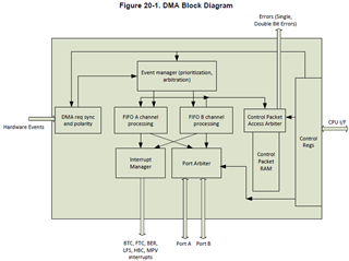
In Technical Reference Manual SPNU563A I found the following information

"20.3.2 Channel Configuration":
"- The RAM is accessible by queue A and queue B state machines as well as CPU."
"- When there are simultaneous accesses, the priority is resolved in a fixed priority scheme with the CPU
having the highest priority."

My questions are:
- Is it a problem with the write or read operation? I need to ensure that all parameters are in place before the DMA transfer trigger.
- Can we estimate the maximum delay value that needs to be applied to ensure that data is in place?
- If applying some do-while() loop fix a problem or just hide it? Could you please describe some background of such behavior?
- From the reference manual it looks like SW access shall have the highest priority so I do not understand why this problem is visible.

Thank you for your help,

Regards,

Sebastian Sokolowski

  • Hi Sebastian Sokolowski,

    Can i get your complete project to test the issue you are talking about?

    --

    Thanks & regards,
    Jagadish.

  • Hello Jagadish,

    Unfortunately, the project code is confidential.

    Now I see that I increased problem reproducibility by increasing timer interrupt frequency and desynchronizing it with the main schedule. Such an approach also increases TX UART traffic so it might be also a case.

    I'm guessing that the "Control Packet RAM" read operation is not atomic. So what will happen when an interrupt is triggered in the middle of this operation?

    Regards,
    Sebastian

  • Hello Jagadish,

    I have some more updates.

    It seems that a timer interrupt triggered during the "Control Packet RAM" reading leads to returning '0' instead of the correct value. With high probability, other interrupts may also affect read operation. 

    I made the following steps to reproduce a problem:
    - generate big TX DMA traffic for 3 UARTS (SCI1, SCI3, SCI4)
    - configure 'RTI1 compare interrupt 0' to the atomic increment of a variable.
    - atomic read of this variable before setting value in the "Control Packet RAM"
    - read this variable again when the problem is observed.

    As a result, I'm observing the incrementation of the variable during data write/read. To get reproduction I need sometimes ~20 minutes of test loop. Now I have 6 reproductions - all with the variable incrementation observed but on different RAM addresses. The second data read seems to return always the correct value so I'm expecting problems with the read operation.

    Regards,
    Sebastian

  • Hello,

    After further tests, I see that the above problems with interrupts are not a root cause but a source of additional fluctuance between hw and sw. 

    What I found out is it is obligatory to use 3 DMA SCI TX channels to reproduce this problem. 2 of them shall be in transmission pending state. According to the below picture, I'm guessing that one is handled by FIFO A, the second by FIFO B and the third is accessing data for configuration purposes using CPU I/F. So we have 3 resources that are trying in parallel to access Control Packet RAM using Control Packet Access Arbiter.

    Could you please verify if from hw perspective such a situation can lead to reading 0 value instead of the correct value on CPU I/F?

    Here is pseudocode which allows me to reproduce this problem:

    #define BUFF_SIZE 128U

    while(true)
    {
        if (false == CheckUartTransmissionPending(Uart1Handler))
        {
            UartWriteDma(Uart1Handler, &buff1[0], BUFF_SIZE);
        }

        if (false == CheckUartTransmissionPending(Uart2Handler))
        {
            UartWriteDma(Uart2Handler, &buff2[0], BUFF_SIZE);
        }

        if (false == CheckUartTransmissionPending(Uart3Handler))
        {
            UartWriteDma(Uart3Handler, &buff3[0], BUFF_SIZE);
        }
    }

    All "DMA Control Packet RAM" write operations in UartWriteDma are done with the following function:

    void WriteAndRead(volatile uint32_t* const pReg, const uint32_t value)
    {
        *pReg = ((uint32_t)value);
        volatile uint32_t actualValue = *pReg;

        if ((actualValue & value) != value)
        {
            ErrorRaise(value, actualValue, *pReg, pReg)
        }
    }

    Regards,

    Sebastian

  • Hello,

    I realize that such behavior most probably is caused by not checking the "Channel Pending Register" before creating a new DMA transfer. Instead of it some bunch of different registers are checked (DMASTAT, BTCFLAG,  HWCHENAR, SWCHENAR).

    When I want to check "Channel Pending Register" I reach a new problem. After the first TX DMA transfer on each UART/DMA channel corresponding bit is in "PEND". I can observe that the transfer is also triggered but  "PEND" bit is not cleared. Below I'm attaching the register state. From my understanding, no action is running but for some reason pending is still set.

    Do you have any idea why the pending bit is not cleared after a successful transfer?

    Regards,
    Sebastian

  • Hi Sebastain,

     The pending bit is set when a hardware request is received independent of HWCHENS or AIM. Let's say you are using the hardware request and the AIM=1, at the end of a block transfer the PEND bit will be clear but to restart the next block the peripheral will still need to generate a hardware DMA request to the DMA module. 

    For more details refer below thread:

    (13) DMA PEND behavior with AIM - Arm-based microcontrollers forum - Arm-based microcontrollers - TI E2E support forums

    --

    Thanks & regards,
    Jagadish.

  • Hello Jagadish,

    I'm not using AIM functionality. As this is a different topic than the original one (most probably related to the wrong synchronization of pending requests) I created a new one with a source code example:

    e2e.ti.com/.../tms570lc4357-channel-pending-register-is-never-cleared-after-the-sci-tx-dma-transfer-is-completed