This thread has been locked.

If you have a related question, please click the "Ask a related question" button in the top right corner. The newly created question will be automatically linked to this question.

LP-AM243: Switching the FSI MUX to access ePWM2

Part Number: LP-AM243
Other Parts Discussed in Thread: SYSCONFIG, AM2434

Hi,

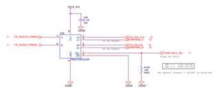
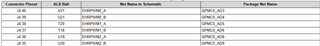
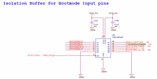
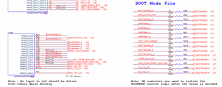
I'm trying to get the signals for EPWM2 channels A and B out to pins 35 and 36 of the Launchpad. I've set GPIO0_28 to HIGH, verified with GPIO_PinOutValue_Read(), but I'm still seeing no PWM signal for ePWM module 2.

Modules 0 and 1 are working fine. What am I missing?

  • I just found this note: "2. The net "FSI/BP_MUX_SEL" is moved from GPMC0_AD13 to GPMC0_AD11."

    Moving to GPIO0_26 has gotten me closer.

    Now the problem is these two channels seem to be entangled. If I change the duty cycle of channel B nothing happens. If I change A to 100%, it will cause both channels to move most of the way there, but I need to also put channel B to 100% for at least channel A to be 100% whereas channel B will only get to ~99%. Is this a hardware problem? EPWM2 has the same sysconfig as EPWM0 and EPWM1 and uses the same interfacing code.

  • Hi Tron, no sure if you are aware, there is a project in MCU-SDK which has 3 EPWM configured (epwm_duty_cycle_sync_am243x-evm_r5fss0-0_nortos_ti-arm-clang). In this project's example.syscfg I don't see any GPIO used for FSI/BP_MUX_SEL though. In any case, please take a look if you haven't. In the meantime, I will try to confirm if there is anything else need it for enabling EPWM2.

    thank you,

    Paula

  • Thanks, Paula. Strangely, the example you mention is configured to use the ALV ball config, not the ALX config the other projects use and that the Launchpad uses. Here's a table from the Launchpad documentation which confirms an ALX chip (SPRUJ12F):

    In my project here are the allocations:
    EPWM0_A: GPMC0_AD3/V21
    EPWM0_B: GPMC0_AD4/U21
    EPWM1_A: GPMC0_AD5/T20
    EPWM1_B: GPMC0_AD6/T18
    EPWM2_A: GPMC0_AD8/U18
    EPWM2_B: GPMC0_AD9/U20

    But here are the allocations in the sync project you've mentioned:
    EPWM0_A: GPMC0_AD3/U20
    EPWM0_B: GPMC0_AD4/U18
    EPWM1_A: GPMC0_AD5/U19
    EPWM1_B: GPMC0_AD6/V20
    EPWM2_A: GPMC0_AD8/V19
    EPWM2_B: GPMC0_AD9/T17

    Could this be why the example code doesn't reference the FSI/EPWM2 MUX pin? I can't currently run it and problem the PWM output to check if it runs on the Launchpad, but the documentation very clearly references a MUX with the FSI header and it did enable me to get some output on the pins, even if not quite right:

    Assuming I'm on the right track, what's the significance of the EPWM2_A and EPWM2_B pins connecting to this boot mode isolator mentioned in PROC109E3_SCH? Could it be something I need to consider to allow the signals to pass through uninterrupted?

    More strangely this document says AM2434 ball U18 and U20 are connected via the bootmode isolation buffer and FSI mux to EPWM2_A and B respectively. Which appears to add weight to the example EPWM sync Sysconfig being the correct configuration, as ALV. The same document does state that it's an ALX chip being referenced:


    But the SPRUJ12F doc states that its U18 and V20 are EPWM2_A and EPWM2_B, which does appear to be backed up by the Sysconfig of my project.

    I don't know what to believe.

  • Hi Tron, ALX and ALV packages has different pins out  (+) [FAQ] AM2432: ALX vs ALV - Arm-based microcontrollers forum - Arm-based microcontrollers - TI E2E support forums

    Our AM243x EVM uses ALV, while our LP uses ALX. I will ask internally if "epwm_duty_cycle_sync_am243x-evm_r5fss0-0_nortos_ti-arm-clang" can be (easily) port it to LP. Apologize if my reference to this example confused you.

    With respect to Bootmode Isolator, this is typically used to isolate boot mode pins of the SoC which have an associated alternate function during normal operation.

    I will try to get a setup on which I can reproduce the issue.

    thank you,

    Paula

  • Hello Tron,

    In EVM, EPWM2 signals are going to HSE or FSI connector there also we have FSI/HSE mux selection line which is controlling either from SOC GPIO and Resistor connected. So, by default this selection pin is connected to Ground through the Resistor. So, EPWM2 pins are selected without controlling any GPIO signal from the SOC. So, this pin configuration is not available in the EVM example to use EPWM2 module.

    Coming to the LP module, again these EPW2 pins are linked with the FSI pins and mentioned by you, after controlling the GPIo0_26 pin as high, as we can drive the EPWM2 signals and again these pins are sharing in between BOOTMODE pins. So, on the side you are driving your PWM signals and another side boot mode it will drive another signals due to this you are not able to drive properly.

    You can try BOOTMODE 8 and BOOT MODE 9 pins as high in your application side for only Testing purpose .

    We don't recommended this procedure but sharing method for Testing purpose .

    You need to control BOOTMODES accordingly to your requirement , otherwise SOC does not enter into proper boot mode.

    Regards,

    S.Anil.

  • Thanks Swargam. I'm only concerned with the LP module.

    Are you saying this note also applies to the E3 revision of the LP?

    I thought that the isolation buffer being a TXB0106PWR in E3 meant that after boot, these balls are still accessible, no? If the balls used for these boot mode signals cannot be accessed reliably by the booster pack pins after boot, what's the significance of having them connected to the booster pack pins at all?

    We've created a comprehensive boosterpack system that relies on 6 EWPM signals. Eventually, we'll do away with the LP altogether but for now, we want to avoid doing PCB layout for the whole AM2434 chip, and I need to find a way to make this work.

    I can't test at this very moment, but I am developing with QSPI boot mode which means BOOTMODE 8 is high and 9 is low, which could explain why EPWM2_A works more than 2_B?

    Where can I find information on how BOOTMODE signals 3-9 are used? I'd like to understand the significance of shifting 8 and 9 to HIGH permanently because it sounds like we need to do this beyond testing, or I need to find a way to switch them HIGH after boot so I can access EPWM2_A and EPWM2_B on the LP without issue.

  • Is this the table I'm looking for?

    Does this mean if I use No Boot, I'm free to set BOOTMODE 8 and 9 to whichever state? But I won't be able to use QSPI boot because we need Iclk to be set?

  • I've been playing with the BOOTMODE switches, but that wasn't the problem. The state of BOOTMODE 8 and 9 have no affect on the EPWM output.

    It turns out no pair of channels were working correctly, not just ePWM2, because I misunderstood the code from the examples - none of which were designed for a different duty cycle signal on the same module. When the config was updated, the lowest value DOWN action would trigger for either channel - I just needed to change the waveform based on which channel was being updated:

        /* Configure Action Qualifier Submodule for asymetric operation */
        aqConfig.zeroAction = EPWM_AQ_ACTION_HIGH;
        aqConfig.prdAction = EPWM_AQ_ACTION_DONOTHING;
        aqConfig.cmpAUpAction = epwmCh ? EPWM_AQ_ACTION_DONOTHING : EPWM_AQ_ACTION_LOW;
        aqConfig.cmpADownAction = EPWM_AQ_ACTION_DONOTHING;
        aqConfig.cmpBUpAction = epwmCh ? EPWM_AQ_ACTION_LOW : EPWM_AQ_ACTION_DONOTHING;
        aqConfig.cmpBDownAction = EPWM_AQ_ACTION_DONOTHING;
        EPWM_aqActionOnOutputCfg(epwmBaseAddr, epwmCh, &aqConfig);

  • Tron, great thanks for letting us know.

    Paula