This thread has been locked.

If you have a related question, please click the "Ask a related question" button in the top right corner. The newly created question will be automatically linked to this question.

MSPM0G1507: Is there any introductions about the instructions cycle counts of MSPM0G1507? I check the instructions cycle counts in debug mode by using SYSTICK but they can not match with the information I get from ARM's web site.

Part Number: MSPM0G1507


Tool/software:

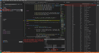
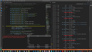
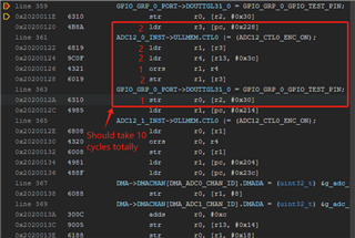
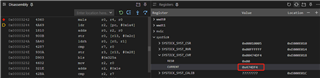
For example, we can see that CPU executes the instruction MULS by taking 4 clock cycles. However, the information came from ARM's web site shows that it takes 1 or 32 clock cycles. Please help comfirm.

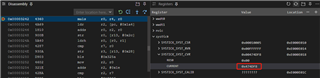
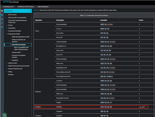
https://developer.arm.com/documentation/ddi0484/c/Programmers-Model/Instruction-set-summary

  • Hi Peter,

    What the CPU rate you are using? I find the ARM documents, it says below:

    So, I want you set the CPU rate as default 32MHz, and then the flash wait state will be zero.

    B.R.

    Sal

  • Hi Peter,

    One thing need correct here.

    Please set CPU run rate smaller than 24MHz for 0 wait state. Maybe you can try 16MHz for simple configuration.

    B.R.

    Sal

  • Hi Peter,

    Not hear the feedback from you for a while, I will close the thread temporarily.

    Feel free to reply the thread if you have further question.

    B.R.

    Sal

  • Hi Sal,

    Sorry for late feedback. I was tracking this issue in E2E chinese site and didn't get your message. I'm using 80MHz CPU rate. So it seems will take 2 CPU clock cycles for the wait state for every instruction, am I right? If yes, the MULS instruction will totally take 3 CPU clock cycles in theory, but 4 CPU clock cycles in fact. I'm still confused about that. Would you please help to figure out it? Thanks.

  • Hi Peter,

    So it seems will take 2 CPU clock cycles for the wait state for every instruction, am I right?

    That is correct. It will take 2 more CPU clock for flash wait.

    the MULS instruction will totally take 3 CPU clock cycles in theory, but 4 CPU clock cycles in fact.

    Firstly, we do NOT maintain the bench test on this, so I can not tell whether this test result following the expectation. [I also think CPU clock =3 is more reasonable, but I can not guarantee this.]

    Secondly, I am not sure how you take the bench test on this, the MSPM0 device do have a Flash Prefetch/Cache. So maybe you test is not accurate.

    I could reccommend antoher test method:

    Set the Assembly Code into the SRAM, and run in the SRAM to see whether the CPU clock consumption is 1. It should be zero wait-state when runing in the SRAM.

    B.R.

    Sal

  • Hi Sal,

    Sad to say, I run the assembly code in SRAM, but the MULS instruction still takes 4 clock cycles.

  • Hi Peter,

    It is weird.

    Let me do some test next week.

    B.R.

    Sal

  • Hi Sal,

    Any updates please?

  • Hi, 

    During debug start and stop, debugger will insert some instruction to M0+ core.

    Maybe this takes some cycles.

    Even if you debug some single-cycle instructions, the result may be 4 systick cycles as well.

    Run 20 times mul, systick down count 26 times.

    Run 10 times mul, systick down count 16 times.

    Run 5 times mul, systick down count 11 times.

    For mul-steps debug, it will takes extra 6 systick cycles depending on this test result.

    I guess for single step debug, it will take 3 extra systick cycles.

    Here is the test demo:

    Instruction_MUL_Test_CycleTest_G3507.zip

    Hope this guide you well.

    Regards,

    Helic

  • Hi Helic,

    Thank you for your explanation. It's quite helpful for me. I check my code by single step debug and find that almost all instructions clock cycles(with taking out the 3 extra clock cycles) conform to the information came from ARM's web site, but only the LDR instruction. The LDR instruction sometimes may takes 3 or 5 clock cycles, just as I mark in red at below screenshot.

    Here's my test code and please kindly help to figure out it.

    instructions_test_demo.zip

    Thank you!

  • Hi, 

    For the extra 3 or 5 clock, or the multi steps debug using breakpoint and resume function's extra 5 clock cycles,

    these phenomena should be caused by debugger, and it will take some time to confirm this.

    Regards,

    Helic

  • Hi, 

    The LDR instruction sometimes may takes 3 or 5 clock cycles, just as I mark in red at below screenshot.

    This is normal because both Resume + breakpoint and Single step debug, need to insert some extra instruction to CPU.

    Regards,

    Helic

  • Hi Helic,

    Even I run the code without debugger, the LDR instruction sometimes still takes 3 ro 5 cycles. And here's my modified test code.

    instructions_test_demo_20250116.zip

    In this code, I add DL_GPIO_togglePins before and after DL_ADC12_enableConversions in line 361, then run the code without debugger. The positive pulse duration is 162.5 or 175ns, equals to 13 or 14 cycles. However, the expected cycle number is 10. According to the test result yesterday, I consider the extra 3 or 4 cycles is taken by instruction LDR R1, [R3].

  • Thanks Helic for backup.

    Hi Peter,

    Sorry for the late response, I am out of office this week. I will follow up for the issue.

    I plan to set up an demo to do experiment and verify it.

    It is expected to update in next Monday.

    B.R.

    Sal

  • Hi Peter,

    I went through the previous reply and your test.

    For GPIO, it is accessed by ULPCLK and MCLK, as shown in the bus organization:

    This might cuase the timing difference for the test. The peripheral sometimes is access by different bus clock.

    So, maybe you can set your MCLK=ULPCLK=40MHz, and test it again.

    B.R.

    Sal

  • Hi Helic,

    Thank you for the update.

    I set MCLK=ULPCLK=40MHz and test again, but it doesn't help. The positive pulse durantion now is 325us, which is equal to 13 clcyes, 3 cycles more than expected. The instruction LDR R1, [R3] still takes 5 cycles, differs from other LDR instructions. 

  • Hi Peter,

    I have done some test. And you are correct, the LDR instruction does have different opeation cycles. 

    - [LDR Rd, ...] The LDR instructions will return the operation value to the Rd register.

    When access different peripheral register, it will take several additional CPU cycles to return the peripheral register value.

    Within my test, for GPIO module, it will take 2 cycles 1 cycle [Update] for LDR instructions; for ADC0 module, it will take 5 cycles for LDR instructions; for SPI0 module, it will take 3 cycles for LDR instructions.

    I suspect below:

    When CPU access the peripheral register, there might have clock sync behavior to make the operation proper, which causes the additional CPU cycles.

    B.R.

    Sal

  • Hi Helic,

    Thanks for your effort. Is there any specification of the accessing register latency which can be shared to me? That will be great helpful to my further study.

  • Hi Peter,

    Sorry, we do NOT maintain related materials for CPU instruction execution.

    I could confirm with the design team, while maybe no addtional information for your reference. Anyway, I will update to you if I got some progress on this topic.

    B.R.

    Sal

  • Hi Peter,

    I do not have the reference materials, while below is my summary on my test:

    For GPIO, there is no latency, and 1 cycles.

    For PD1 (MCLK), there is 1 additional cycles latency, and is total 3 cycles.

    For PD0 (ULPCLK), there is 3 additional cycles latency, and is total 5 cycles.

    B.R.

    Sal

  • By the way, I would like to know what is your concerning here for the CPU instruction cycles, Is the application really restricted on the CPU timing? Thanks.

  • Hi Sal,

    Yes. In my project, the performance is strongly corelated with the code execution speed. Anyway, thank you for your research.