Part Number: MSPM0G3507
Tool/software:
Hello experts,
I'have to develop a comunication via SPI + DMA from MSPM0G3507 to a FRAM (MB85RS256B). Page 9 of the FRAM's datasheet has the text ..."Risen CS will terminate the WRITE command. However if you continue sending the writing data for 8 bits each before CS rising, it is possible to continue writing with automatic address increment".
I'm able to write and read individual values to/from the FRAM without the DMA.
Well, I started to use the example spi_controller_repeated_fifo_dma_interrupts_LP_MSPM0G3507_nortos_ticlang, the only change I did was: SPI clock, SPI pins, and setting a 3-wire SPI (controlling CS using the GPIO). I keept all the DMA configuration.
Citing Bruce McKenney, I understand that "SPI is intrinsically full-duplex -- for every byte you transmit, you receive one; and, as in this case, if you want to receive a byte you must send one. We refer to "transmit only" and "receive only" transactions, but those only mean that the other end isn't interested in what the data is."
My application will need to write and read a big chunk of data but for now I'm doing tests with 30 samples (baby steps). So, I separete my code in 2 parts:
Part 1) write data to FRAM: I adapted gTxPacket to incorporate the op-codes (WREN and WRITE), start address and the data that needs to be written. Also, gTxPacket is in a one-byte format (uint8_t).
I'm not interested in data coming from the RXFIFO, its trash.
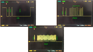
The write part looks okay, I have a timer which counts 1s for the start of transfer. I checked CS, CLK, and PICO on an oscilloscope. CLK is pretty hard to see, CS is lasting ~16us at low and I know that to write 16 bits without DMA takes ~6.6us.
Part 2) read data from FRAM: I adapted gTxDummy to incorporate the op-code (READ), start address and the dummy data that needs to be written in order to generate the clocks. Also, gTxDummy is in a one-byte format (uint8_t).
The read part does not look okay. I'm VERY interested in the data coming from the RXFIFO but when I check my gRxPacket, it has 255 (0xFF) in every position (I cleared it at the begin of the main()). It should have the same content as gTxPacket.
void SPI_send(void)
{
    // Part 1: writing data to FRAM

    /*
     * Configure DMA source, destination and size to transfer data from
     * gTxPacket to TXDATA. The DMA transfer will start when TX interrupt is
     * set, which it should already be set (which indicates that the SPI is
     * ready to transfer) so the DMA will begin this transfer when the channel
     * is enabled.
     */
    DL_DMA_setSrcAddr(DMA, DMA_CH0_CHAN_ID, (uint32_t) &gTxPacket[0]);
    DL_DMA_setDestAddr(DMA, DMA_CH0_CHAN_ID, (uint32_t)(&SPI_0_INST->TXDATA));
    DL_DMA_setTransferSize(
        DMA, DMA_CH0_CHAN_ID, sizeof(gTxPacket) / sizeof(gTxPacket[0]));

    /*
     * Configure DMA source, destination and size from RXDATA to gRxPacket.
     * The DMA transfer will start when the RX interrupt is set, which happens
     * when the device receives data.
     */
    DL_DMA_setSrcAddr(DMA, DMA_CH1_CHAN_ID, (uint32_t)(&SPI_0_INST->RXDATA));
    DL_DMA_setDestAddr(DMA, DMA_CH1_CHAN_ID, (uint32_t) &gRxPacket[0]);
    DL_DMA_setTransferSize(DMA, DMA_CH1_CHAN_ID, ARRAY_SIZE);

    DL_GPIO_clearPins(GPIO_PORT, GPIO_CS_SPI_PIN);

    /*
     * The SPI TX interrupt is already set, indicating the SPI is ready to
     * transmit data, so enabling the DMA will start the transfer
     */
    DL_DMA_enableChannel(DMA, DMA_CH0_CHAN_ID);
    DL_DMA_enableChannel(DMA, DMA_CH1_CHAN_ID);

    /*
     * Wait in SLEEP mode until SPI_PACKET_SIZE bytes have been transferred
     * from gTxPacket to the SPI TXFIFO, and the DMA interrupt is triggered
     */
    while (false == isDMATXDataTransferred) {
        __WFE();
    }

    /*
     * Wait until the SPI has transmitted all the data and the TXFIFO
     * is empty
     */
    while (false == isSPIDataTransmitted) {
        __WFE();
    }

    /*
     * Wait in SLEEP mode until SPI_PACKET_SIZE bytes have been transferred
     * from SPI TXFIFO to gRxPacket, and the DMA interrupt is triggered
     */
    while (false == isDMARXDataTransferred) {
        __WFE();
    }

    /*
     * Optional SW breakpoint to check results.
     * If this example is used with the
     * spi_peripheral_repeated_fifo_dma_interrupts example,
     * the expected data that will be received in gRxPacket is
     * {'x', 0x2, 0x3, 0x4}, where 'x' starts at 0x0 and
     * should increment every time the Peripheral example
     * sends a new data packet.
     */
    //        __BKPT(0);

    isSPIDataTransmitted   = false;
    isDMATXDataTransferred = false;
    isDMARXDataTransferred = false;

    DL_GPIO_setPins(GPIO_PORT, GPIO_CS_SPI_PIN);

    // Part 2: reading data from FRAM

    // Sugestion from Chris https://e2e.ti.com/support/microcontrollers/arm-based-microcontrollers-group/arm-based-microcontrollers/f/arm-based-microcontrollers-forum/1439766/mspm0g3507-cant-get-spi-to-automatically-clock-in-receive-data-in-dma-mode

    /*
     * Configure DMA source, destination and size to transfer data from
     * tx_pbuf to TXDATA. The DMA transfer will start when TX interrupt is
     * set, which it should already be set (which indicates that the SPI is
     * ready to transfer) so the DMA will begin this transfer when the channel
     * is enabled.
     */
    DL_DMA_setSrcAddr(DMA, DMA_CH0_CHAN_ID, (uint32_t) &gTxDummy[0]);
    DL_DMA_setDestAddr(DMA, DMA_CH0_CHAN_ID, (uint32_t)(&SPI_0_INST->TXDATA));
        DL_DMA_setTransferSize(
        DMA, DMA_CH0_CHAN_ID, sizeof(gTxDummy) / sizeof(gTxDummy[0]));

    NVIC_EnableIRQ(SPI_0_INST_INT_IRQN);

    // enable chip select
    DL_GPIO_setPins(GPIO_PORT, GPIO_CS_SPI_PIN);

    /*
     * The SPI TX interrupt is already set, indicating the SPI is ready to
     * transmit data, so enabling the DMA will start the transfer
     */
    DL_DMA_enableChannel(DMA, DMA_CH0_CHAN_ID);

    /*
     * Wait in SLEEP mode until SPI_PACKET_SIZE bytes have been transferred
     * from tx_pbuf to the SPI TXFIFO, and the DMA interrupt is triggered
     */
    while (false == isDMATXDataTransferred) {
        __WFE();
    }

    /*
     * Wait until the SPI has transmitted all the data and the TXFIFO
     * is empty
     */
    while (false == isSPIDataTransmitted) {
        __WFE();
    }

    // dummy read clears spi data waiting interrupt caused by spi tx
    DL_SPI_receiveData8(SPI_0_INST);

    /*
     * Configure DMA source, destination and size from RXDATA to rx_pbuf.
     * The DMA transfer will start when the RX interrupt is set, which happens
     * when the device receives data.
     */
    DL_DMA_setSrcAddr(DMA, DMA_CH1_CHAN_ID, (uint32_t)(&SPI_0_INST->RXDATA));
    DL_DMA_setDestAddr(DMA, DMA_CH1_CHAN_ID, (uint32_t) &gRxPacket[0]);
    DL_DMA_setTransferSize(DMA, DMA_CH1_CHAN_ID, ARRAY_SIZE);
    DL_DMA_enableChannel(DMA, DMA_CH1_CHAN_ID);

    /*
     * Wait in SLEEP mode until SPI_PACKET_SIZE bytes have been transferred
     * from SPI TXFIFO to rx_pbuf, and the DMA interrupt is triggered
     */
    /*while ((false == gDMARXDataTransferred) && (ARRAY_SIZE > 0)) {
        // generates sclks until ARRAY_SIZE requested number of bytes have been read
        DL_SPI_transmitData8(SPI_0_INST, 0x00);
    }*/
}

void SPI_0_INST_IRQHandler(void)
{
    switch (DL_SPI_getPendingInterrupt(SPI_0_INST)) {
        case DL_SPI_IIDX_DMA_DONE_TX:
            /* DMA is done transferring data from gTxPacket to TXFIFO */
            isDMATXDataTransferred = true;
            break;
        case DL_SPI_IIDX_TX_EMPTY:
            /* SPI is done transmitting data and TXFIFO is empty */
            isSPIDataTransmitted = true;
            break;
        case DL_SPI_IIDX_DMA_DONE_RX:
            /* DMA is done transferring data from RXFIFO to gRxPacket*/
            isDMARXDataTransferred = true;
        default:
            break;
    }
}
I looked into other post here (e2e.ti.com/.../mspm0g3507-cant-get-spi-to-automatically-clock-in-receive-data-in-dma-mode). I implemented it, but the solution Chris kindly suggested is not working either.
I also checked:
e2e.ti.com/.../mspm0g3507-dma-enabled-spi-communication-with-ads8684a
e2e.ti.com/.../mspm0g3507-spi-dma-receive-abnormal
e2e.ti.com/.../ads1258-ep-using-dma-with-ads1258
Please, could someone give me any advice or suggestion to fix my reading part of the code?
Thanks,
Andrea