This thread has been locked.

If you have a related question, please click the "Ask a related question" button in the top right corner. The newly created question will be automatically linked to this question.

MSPM0G3507: Duty cycle of first pwm period using shadow compare?

Part Number: MSPM0G3507

Tool/software:

Hey.
I am working setting up some center aligned pwm signals, and are setting it up for using the shadow compare feature, to only update the compare value on a ZERO event.

It works fine, but there is one oddity:

The very first duty cycle seems to have an arbitrary length that I cannot seem to change. After the first pulse, things work fine, but no matter which order I write the registers, the first pulse seem unaffected.

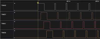
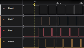
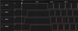
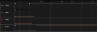
Here's a screenshot with an initial duty cycle set up for 10% showing the issue:

  • Hi,

    Interesting behavior. Could you send your project here, so we can run a test on it and check. 

    Best regards,

    Cash Hao

  • You should probably call DL_Timer_setCaptureCompareValue() before calling DL_Timer_setCaptCompUpdateMethod(). Since  CCUPD is initially 0 (bypass shadow), the set will happen immediately.

  • Setting the compare value before engaging the shadow compare functionaity does make sense, and I did try that. But I didnt get the expected results.
    Here's the current setup, engaging shadow compare/load BEFORE setting load/compare values:


    And here, AFTER setting load/compare values:


    I can't quite figure out why the pins stay high that long in the second image....
    I am setting things up a bit manually - here's the function I use for it - there's quite a bit debugging going on, but you can see the order I set things up in:

    void PWM_init()
    {
        // ===================================== 1 - Configure timer clocking =================================
        // Set the timer clock = busclk (80MHZ)
        static DL_TimerA_ClockConfig pwmClockConfig = {
            .clockSel = DL_TIMER_CLOCK_BUSCLK,
            .divideRatio = DL_TIMER_CLOCK_DIVIDE_1,
            .prescale = 0U};
    
    // !!!!!!! Slow debugging !!!!!!!!!!!!!!!!!!!
    pwmClockConfig.divideRatio = DL_TIMER_CLOCK_DIVIDE_8;
    pwmClockConfig.prescale = 99U;
    // !!!!!!!!!!!!!!!!!!!!!!!!!!!!!!!!!!!!!!!!!!!!!!!!!!!!!
    
        DL_Timer_setClockConfig(TIMA0, &pwmClockConfig);
        DL_Timer_setClockConfig(TIMG7, &pwmClockConfig);
        DL_Timer_setClockConfig(TIMG6, &pwmClockConfig);
        DL_Timer_setClockConfig(TIMA1, &pwmClockConfig);
    
        // ============================== 2 - CCACT - Capture/Compare Action ==================================
        // Raise CC pin on CompareUp, lower on CompareDown. (Center aligned pwm)
        uint32_t actions = (DL_TIMER_CC_CUACT_CCP_HIGH | DL_TIMER_CC_CDACT_CCP_LOW);
        DL_Timer_setCaptureCompareAction(TIMA0, actions, DL_TIMER_CC_0_INDEX);
        DL_Timer_setCaptureCompareAction(TIMG7, actions, DL_TIMER_CC_0_INDEX);
        DL_Timer_setCaptureCompareAction(TIMG6, actions, DL_TIMER_CC_0_INDEX);
        DL_Timer_setCaptureCompareAction(TIMA1, actions, DL_TIMER_CC_0_INDEX);
    
        // ============================ 3 - CCCTL - Capture/Compare Control ===================================
        // TIMA0: channel 0 = pwm1 / channel 1 used to trigger TIMG7 (pwm2)
        // TIMA1: channel 0 = pwm3 / channel 1 used to trigger TIMG6 (pwm4)
    
        // Set up bitmask to exclude reserved bits. 
        uint32_t ccctl_mask = (GPTIMER_CCCTL_01_CC2SELD_MASK | 
                                    GPTIMER_CCCTL_01_CCACTUPD_MASK |
                                    GPTIMER_CCCTL_01_SCERCNEZ_MASK |
                                    GPTIMER_CCCTL_01_CC2SELU_MASK |
                                    GPTIMER_CCCTL_01_CCUPD_MASK |
                                    GPTIMER_CCCTL_01_COC_MASK |
                                    GPTIMER_CCCTL_01_ZCOND_MASK | 
                                    GPTIMER_CCCTL_01_LCOND_MASK | 
                                    GPTIMER_CCCTL_01_ACOND_MASK |
                                    GPTIMER_CCCTL_01_CCOND_MASK);
    
        // Another bitmask for our chosen bits
        uint32_t ccctl_config = (GPTIMER_CCCTL_01_COC_COMPARE |         // Use compare mode
                                GPTIMER_CCCTL_01_ZCOND_CC_TRIG_NO_EFFECT |
                                GPTIMER_CCCTL_01_LCOND_CC_TRIG_NO_EFFECT |
                                GPTIMER_CCCTL_01_ACOND_TIMCLK |
                                GPTIMER_CCCTL_01_CCOND_NOCAPTURE |
                                GPTIMER_CCCTL_01_CCUPD_IMMEDIATELY); 
    
        DL_Common_updateReg(&TIMA0->COUNTERREGS.CCCTL_01[0], ccctl_config, ccctl_mask);
        DL_Common_updateReg(&TIMA0->COUNTERREGS.CCCTL_01[1], ccctl_config, ccctl_mask);
        DL_Common_updateReg(&TIMA1->COUNTERREGS.CCCTL_01[0], ccctl_config, ccctl_mask);
    
        // Set the remainig timer channels up to generate ZERO pulse, on rising trigger edge.
        ccctl_config |= GPTIMER_CCCTL_01_ZCOND_CC_TRIG_RISE;                     
        DL_Common_updateReg(&TIMG7->COUNTERREGS.CCCTL_01[0], ccctl_config, ccctl_mask);               
        DL_Common_updateReg(&TIMG6->COUNTERREGS.CCCTL_01[0], ccctl_config, ccctl_mask);
        DL_Common_updateReg(&TIMA1->COUNTERREGS.CCCTL_01[0], ccctl_config, ccctl_mask);
    
        // // Set up for shadow compare (only apply change to compare value (duty cycle) after completing a cycle.)
        // TIMA0->COUNTERREGS.CCCTL_01[0] |= DL_TIMER_CC_UPDATE_METHOD_ZERO_EVT;
        // TIMA1->COUNTERREGS.CCCTL_01[0] |= DL_TIMER_CC_UPDATE_METHOD_ZERO_EVT;
        // TIMG7->COUNTERREGS.CCCTL_01[0] |= DL_TIMER_CC_UPDATE_METHOD_ZERO_EVT;
        // TIMG6->COUNTERREGS.CCCTL_01[0] |= DL_TIMER_CC_UPDATE_METHOD_ZERO_EVT;
        // TIMA0->COUNTERREGS.CCCTL_01[1] |= DL_TIMER_CC_UPDATE_METHOD_ZERO_EVT;
        // TIMA1->COUNTERREGS.CCCTL_01[1] |= DL_TIMER_CC_UPDATE_METHOD_ZERO_EVT;
    
        // // Enable shadow load - only update LOAD value on zero events.
        // TIMA0->COMMONREGS.GCTL = GPTIMER_GCTL_SHDWLDEN_ENABLE;
        // TIMA1->COMMONREGS.GCTL = GPTIMER_GCTL_SHDWLDEN_ENABLE;
        // TIMG7->COMMONREGS.GCTL = GPTIMER_GCTL_SHDWLDEN_ENABLE;
        // TIMG6->COMMONREGS.GCTL = GPTIMER_GCTL_SHDWLDEN_ENABLE;
    
        // =========================== 4 - OCTL - Capture/Compare Output Control ==============================
        uint32_t init_val = DL_TIMER_CC_OCTL_INIT_VAL_LOW;     // Initial output low.
        uint32_t octl_inv = DL_TIMER_CC_OCTL_INV_OUT_DISABLED; // Non-inverted output
        uint32_t function = DL_TIMER_CC_OCTL_SRC_FUNCVAL;      // Use signal gen. output
        DL_Timer_setCaptureCompareOutCtl(TIMA0, init_val, octl_inv, function, DL_TIMER_CC_0_INDEX);
        DL_Timer_setCaptureCompareOutCtl(TIMG7, init_val, octl_inv, function, DL_TIMER_CC_0_INDEX);
        DL_Timer_setCaptureCompareOutCtl(TIMG6, init_val, octl_inv, function, DL_TIMER_CC_0_INDEX);
        DL_Timer_setCaptureCompareOutCtl(TIMA1, init_val, octl_inv, function, DL_TIMER_CC_0_INDEX);
    
        // ============================== 5 - IFCTL - Input (Filter) Control ==================================
        uint32_t ifctl_inv = GPTIMER_IFCTL_01_INV_NOINVERT;     // No input inversion (INV)
        uint32_t ifctl_slct = GPTIMER_IFCTL_01_ISEL_TRIG_INPUT; // Input select (ISEL) - use trigger
        DL_Timer_setCaptureCompareInput(TIMG7, ifctl_inv, ifctl_slct, DL_TIMER_CC_0_INDEX);
        DL_Timer_setCaptureCompareInput(TIMG6, ifctl_inv, ifctl_slct, DL_TIMER_CC_0_INDEX);
        DL_Timer_setCaptureCompareInput(TIMA1, ifctl_inv, ifctl_slct, DL_TIMER_CC_0_INDEX);
    
        // ============================= 6 - LOAD value (PWM Period/Frequency) ================================
        // uint32_t pwm_load_value = calc_pwm_load_value(PWM_FREQUENCY, BUSCLK_FREQ);  // Note PD1 = 80MHZ, PD0 = 40MHz
        // OVERRIDE FOR NOW
        pwm_load_value = (1667 >> 1); // half-ing because of center-aligned pwm
    
    // !!!!!!!!!!!!! SLOW FOR DEBUGGING !!!!!!!!!!!!!!!!!!!!!!!!!!!!!!!
    pwm_load_value = 2000;
    //!!!!!!!!!!!!!!!!!!!!!!!!!!!!!!!!!!!!!!!!!!!!!!!!!!!!!!!!!!!!!!!!!!!!
    
        DL_Timer_setLoadValue(TIMA0, pwm_load_value);
        DL_Timer_setLoadValue(TIMG7, pwm_load_value);
        DL_Timer_setLoadValue(TIMG6, pwm_load_value);
        DL_Timer_setLoadValue(TIMA1, pwm_load_value);
    
        // ================================= 7 - CTRCTL - Counter Control =====================================
        uint32_t ctrctl_mask = (GPTIMER_CTRCTL_CZC_MASK | GPTIMER_CTRCTL_CAC_MASK |
                                GPTIMER_CTRCTL_CLC_MASK | GPTIMER_CTRCTL_CVAE_MASK |
                                GPTIMER_CTRCTL_CM_MASK | GPTIMER_CTRCTL_REPEAT_MASK |
                                GPTIMER_CTRCTL_EN_MASK);
        uint32_t ctrctl_config = (GPTIMER_CTRCTL_REPEAT_REPEAT_1 | GPTIMER_CTRCTL_CM_UP_DOWN |
                                  GPTIMER_CTRCTL_EN_DISABLED | GPTIMER_CTRCTL_CVAE_ZEROVAL |
                                  GPTIMER_CTRCTL_CZC_CCCTL0_ZCOND | GPTIMER_CTRCTL_CAC_CCCTL0_ACOND |
                                  GPTIMER_CTRCTL_CLC_CCCTL0_LCOND);
    
        // TIMG7, TIMG6 and TIMA1 are not enabled here - they are triggered by TIMA0.
        // Only enable TIMA0 after everything is set up.
        DL_Common_updateReg(&TIMG7->COUNTERREGS.CTRCTL, ctrctl_config, ctrctl_mask);
        DL_Common_updateReg(&TIMG6->COUNTERREGS.CTRCTL, ctrctl_config, ctrctl_mask);
        DL_Common_updateReg(&TIMA1->COUNTERREGS.CTRCTL, ctrctl_config, ctrctl_mask);
    
        // ================================ 8 - DUTY CYCLES (COMPARE VALUE) ===================================
        // Set CC1 for TIMA0/1 to 50%, for handling phase.
        TIMA0->COUNTERREGS.CC_01[1] = 417;
        TIMA1->COUNTERREGS.CC_01[1] = 417;
    
    // !!!!!!!!!!!!!!!!!!!!!!!!!!!! DEBUGGING !!!!!!!!!!!!!!!!!!!!!!!
    TIMA0->COUNTERREGS.CC_01[1] = 1000;
    TIMA1->COUNTERREGS.CC_01[1] = 1000;
    // !!!!!!!!!!!!!!!!!!!!!!!!!!!!!!!!!!!!!!!!!!!!!!!!!!!!!!!!!!!!!!!!!
    
        // LOAD = 1667 / 2 = 100%
        // 10% = LOAD - LOAD / 100 * 10
        uint32_t initial_duty_cycle = pwm_load_value - ((pwm_load_value / 100) * INITIAL_DUTY_CYCLE); // 1%  // 750; // about 10%
        TIMA0->COUNTERREGS.CC_01[0] = initial_duty_cycle;
        TIMG7->COUNTERREGS.CC_01[0] = initial_duty_cycle;
        TIMG6->COUNTERREGS.CC_01[0] = initial_duty_cycle;
        TIMA1->COUNTERREGS.CC_01[0] = initial_duty_cycle;
    
        // Update global variable.
        current_duty_cycle = INITIAL_DUTY_CYCLE;
    
    
    //!!!!!!!!!!!!!!!!!!!!!!!!!!!!!!!!!!!!!!!!!!!!!!!!!!!!!!!!!!!!!!!!!!!!!!!!!!!!!!!!!!!!!!!!!!!!!!!!!!!!
        TIMA0->COUNTERREGS.CCCTL_01[0] |= DL_TIMER_CC_UPDATE_METHOD_ZERO_EVT;
        TIMA1->COUNTERREGS.CCCTL_01[0] |= DL_TIMER_CC_UPDATE_METHOD_ZERO_EVT;
        TIMG7->COUNTERREGS.CCCTL_01[0] |= DL_TIMER_CC_UPDATE_METHOD_ZERO_EVT;
        TIMG6->COUNTERREGS.CCCTL_01[0] |= DL_TIMER_CC_UPDATE_METHOD_ZERO_EVT;
    
    TIMA0->COUNTERREGS.CCCTL_01[1] |= DL_TIMER_CC_UPDATE_METHOD_ZERO_EVT;
    TIMA1->COUNTERREGS.CCCTL_01[1] |= DL_TIMER_CC_UPDATE_METHOD_ZERO_EVT;
    
        // Enable shadow load - only update LOAD value on zero events.
        TIMA0->COMMONREGS.GCTL = GPTIMER_GCTL_SHDWLDEN_ENABLE;
        TIMA1->COMMONREGS.GCTL = GPTIMER_GCTL_SHDWLDEN_ENABLE;
        TIMG7->COMMONREGS.GCTL = GPTIMER_GCTL_SHDWLDEN_ENABLE;
        TIMG6->COMMONREGS.GCTL = GPTIMER_GCTL_SHDWLDEN_ENABLE;
    //!!!!!!!!!!!!!!!!!!!!!!!!!!!!!!!!!!!!!!!!!!!!!!!!!!!!!!!!!!!!!!!!!!!!!!!!!!!!!!!!!!!!!!!!!!!!!!!!!!!!!!
    
        // ======================================= 9 - ENABLE EVENTS =========================================
        // These are used to trigger pwm-2/3 (TIMG7/TIMG6)
        // PWM 2 & 3 are triggered by compare-up events from TIMA0 and TIMA1 respectively -
        TIMA0->GEN_EVENT0.IMASK |= DL_TIMER_EVENT_CC1_UP_EVENT; // Triggers TIMG7
        TIMA1->GEN_EVENT0.IMASK |= DL_TIMER_EVENT_CC1_UP_EVENT; // Triggers TIMG6
    
        // Triggers for ADC0 (CCU/CCD/ZERO/LOAD)
        TIMA0->GEN_EVENT1.IMASK |= (DL_TIMER_EVENT_CC1_UP_EVENT |
                                    DL_TIMER_EVENT_CC1_DN_EVENT |
                                    DL_TIMER_EVENT_LOAD_EVENT |
                                    DL_TIMER_EVENT_ZERO_EVENT);
    
    // DEBUGG!!!!!!!!!!!!!!!!!!!!!!!!!!!!!!!!!!!!!!!!!!!!!!!!!!!!!!
    TIMA1->GEN_EVENT1.IMASK |= (DL_TIMER_EVENT_CC1_UP_EVENT);
    //!!!!!!!!!!!!!!!!!!!!!!!!!!!!!!!!!!!!!!!!!!!!!!!!!!!!!!!!!!!!!
    
        // Also set up an interrupt for the CCU1 event of TIMA0 - this must only fire once, and is used to
        // enable the ADC to start it's sampling at the right event.
        TIMA0->CPU_INT.IMASK = DL_TIMER_EVENT_CC1_UP_EVENT;
    
    
        // =================================== 10 - CONFIGURE CROSS-TRIGGER ===================================
        DL_Timer_configCrossTrigger(TIMA0,
                                    DL_TIMER_CROSS_TRIG_SRC_LOAD,         // LOAD event cross-trigger TIMA1 (180 degree phase shift)
                                    DL_TIMER_CROSS_TRIGGER_INPUT_ENABLED, // Enable source
                                    DL_TIMER_CROSS_TRIGGER_MODE_ENABLED); // Enable Cross trigger output
    
        // ================================== 11 - SELECT EXTERNAL TRIGGER EVENT ===============================
        DL_TimerG_setExternalTriggerEvent(TIMG7, GPTIMER_TSEL_ETSEL_TRIG_SUB0); // Select subscriber 0 as trigger
        DL_TimerG_setExternalTriggerEvent(TIMG6, GPTIMER_TSEL_ETSEL_TRIG_SUB0); // Same
        DL_TimerA_setExternalTriggerEvent(TIMA1, GPTIMER_TSEL_ETSEL_TRIG0);     // Select trigger input 0 as trigger.
    
        // ====================================== 12 - SET PUBLISHER EVENT CHs =================================
        TIMA0->FPUB_0 = 1; // Trigger TIMG7 on CC1 up event
        TIMA1->FPUB_0 = 2; //
        TIMA0->FPUB_1 = 3; // Trigger events for ADC
    
    // !!!!!!!!!!!!!!!!DEBUG !!!!!!!!!!!!!!!!!!!!!!!!!!!
    TIMA1->FPUB_1 = 5;
    //!!!!!!!!!!!!!!!!!!!!!!!!!!!!!!!!!!!!!!!!!!!!!!!!!
    
        // ===================================== 13 - SET SUBSCRIBER EVENT CHs =================================
        TIMG7->FSUB_0 = 1;
        TIMG6->FSUB_0 = 2;
    
        // ==================================== 14 - SET CC PIN DIRECTION =====================================
        TIMA0->COMMONREGS.CCPD = GPTIMER_CCPD_C0CCP0_OUTPUT;
        TIMG7->COMMONREGS.CCPD = GPTIMER_CCPD_C0CCP0_OUTPUT;
        TIMG6->COMMONREGS.CCPD = GPTIMER_CCPD_C0CCP0_OUTPUT;
        TIMA1->COMMONREGS.CCPD = GPTIMER_CCPD_C0CCP0_OUTPUT;
    
        // =================================== 15 - ENABLE EXTERNAL TRIGGER ===================================
        DL_TimerG_enableExternalTrigger(TIMG7);
        DL_TimerG_enableExternalTrigger(TIMG6);
        DL_TimerG_enableExternalTrigger(TIMA1);
    
        // ==================================== 16 - ENABLE TIMER CLOCK ========================================
        DL_TimerG_enableClock(TIMG7);
        DL_TimerG_enableClock(TIMG6);
        DL_TimerA_enableClock(TIMA1);
        DL_TimerA_enableClock(TIMA0);
    
        // ================================= 17 - ENABLE PWMs, START TIMA0 =====================================
    
        ctrctl_config |= GPTIMER_CTRCTL_EN_ENABLED;
        DL_Common_updateReg(&TIMA0->COUNTERREGS.CTRCTL, ctrctl_config, ctrctl_mask);
    }


  • Hi,

    I will look into this code first. Just for check is it possible to directly provided the project here?

    Best regards,

    Cash Hao

  • As you can see in the code, I am currently testing things out, using the systick to generate an interrupt to change load and compare value.
    Interestingly, if I dont make any change to those, but only stick with initial values, and enable shadow-registers after setting load/compare values, I get this;


  • Interestingly, I think I found something that works, in these steps:

    1) Set initial compare and load values.
    2) Enable shadow functionality.
    3) Set the initial compare and load values AGAIN.

    I just wonder if it makes sense that I have to set them both before and after enabling shadow register?

  • Hi,

    Well, I do not think it requires to set the initial compare and load values two times. Let me run some tests tomorrow and check on this behavior. 

    Best regards,

    Cash Hao 

  • It's true that TRM Table 27-16, for entry "0", doesn't mention "stored in a shadow compare register". It never occurred to me that it wasn't set (immediately) Through the shadow register. 

    Good catch.

  • Hi,

    I do observe this behavior on my side.

    The issue is gone when I set the CC value again after enabling shadow function. No need to set load value again here. 

    So, the current solution would be set the CC value twice before and after enable shadow function.

    Best regards,

    Cash Hao