This thread has been locked.

If you have a related question, please click the "Ask a related question" button in the top right corner. The newly created question will be automatically linked to this question.

LP-AM263P: CMPSS Hardware Configuration

Part Number: LP-AM263P
Other Parts Discussed in Thread: SYSCONFIG

Tool/software:

Hi

I'm reviewing AM263Px TI's technical reference manual for the CMPSS module, and I've come across two block diagrams. There are a few points I'm unsure about.

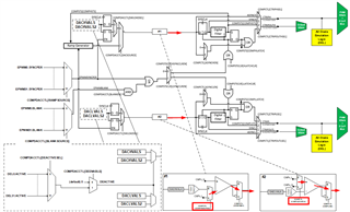
First, can the positive input of CompH and the negative input of CompL be configured? Or are they directly hardwired to the ADC input pins? Is it possible to configure either of them to use a fixed 3.3V reference? If so, how can that be done? Both COMPHSOURCE and COMPLSOURCE are only 1-bit wide, and I couldn't find any setting in SysConfig that allows selecting a 3.3V reference.

Second, in the block diagram, the COMPLSOURCE bit appears to control the negative input of COMPL. However, based on my review of the SysConfig options and the register documentation, it seems like it should be selecting the positive input instead. Has there possibly been a mistake in the diagram?
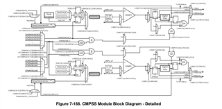


Regards,
Burak


  • negative input of COMPL are connected DAC module directly? Is this configurable?

  • Hey Burak,

    I think we need to make some updates to these block diagrams. Where did you find the first block diagram you shared?

    The second diagram from the TRM will need to be updated. I am attaching a diagram that properly described the CMPSSA High and Low Comparator controls.

    1) The +Input of CompH is hardwired to the ADC/Analog pin input and the -Input of CompL is hardwired to the 12-bit DACL output. The first diagram you shared presents some additional options that are not actually present. As you noted the COMPxSOURCE bitfield is only a single bit. The only option here would be to program the DACL output to its max value which would correlate to either VDDA3V3-50mV or 33/18*VDACREF depending on which reference is configured for the DAC (VDDA3V3 or VDACREF respectively).

    2) You are correct that the COMPLSOURCE bit controls the positive input of COMPL. I have put red boxes/arrows around the relevant content in the diagram below.

    I will file a bug to have this diagram fixed in the next release.

    In regard to your response thread: Yes, the -Input of CompL is connected the 12-bit DACL which is configurable by the DAVLVALA register. This could be configured to output a value comparable to 3.3V as defined in response2 above.

    Best Regards,

    Zackary Fleenor