This thread has been locked.

If you have a related question, please click the "Ask a related question" button in the top right corner. The newly created question will be automatically linked to this question.

AM2434: Question about OSPI-READ half-level (Continue)

Part Number: AM2434
Other Parts Discussed in Thread: SK-AM64B, SYSCONFIG

Tool/software:

A few months ago, we push a question on the forum regarding the issue of half-level signals when reading flash data via OSPI, as detailed in this link:

e2e.ti.com/.../5739028

The topic has since been automatically closed, but we never received a clear explanation of the root cause or an effective solution to the problem.

We recently conducted further testing using the EVM board and SDK examples. The issue can be reliably reproduced following the steps below. We hope TI's experts can continue analyzing this problem to determine its root cause and explore potential solutions.

1.  Import the SDK example project: "mcu_plus_sdk_am243x_11_00_00_15\examples\drivers\ospi\ospi_flash_dma\am243x-evm"

2. Unckeck "Enable PHY Mode" on example.syscfg->OSPI

3. Modify ospi_flash_dma.c file to fill the gOspiFlashDmaTxBuf array with all 0xFF

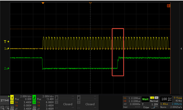
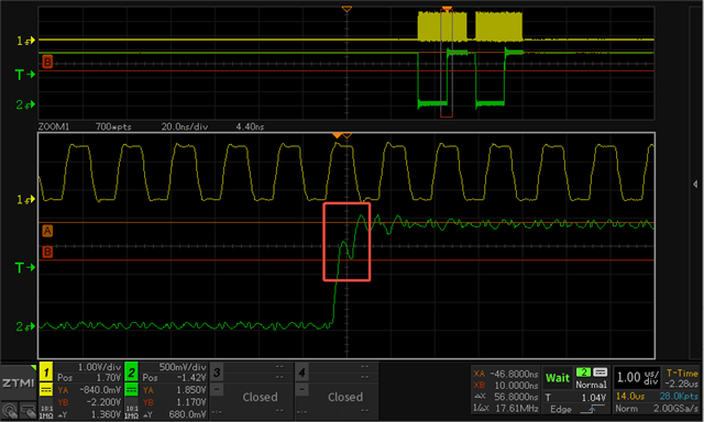
4. Debug the project and set a breakpoint at ospi_flash_dma.c:123.  Using an oscilloscope to capture the waveforms of OSPI_CLK and OSPI_DQ4.

5. Continue runing the project and we can capture the half-level waveform for OSPI-READ. 1=CLK, 2=DQ4
  • Hi Liang,

    Can you please try with the following setting. Change the clock divider to the value 8.

    Earlier:

    So, for 166 MHZ / 4 = 41 MHz the dummy cycles required for command is 4.

    Now:

    But for 166 MHz / 8 = 20 MHz the dummy cycles required for command is just 3.

    Hence, in SysConfig under Flash you would need to change dummy cycles command to 3 and the read id dummy cycles for octal mode as 3.

    Values to edit Dummy Clocks (CMD) -> 3 and Number Of Dummy Cycles In Octal Mode -> 3. Clock Divider to 8.

    Have Controller and Flash dummy cycles read same as 24 itself.

    Give your application a free run without any register modification(as I mentioned earlier), and let me know if you see any half level issue now?

    Anastas, tried the same and did not see any half level issue.

    If you do not see the issue, then we can go ahead with the changes in the SDK and put this change of:

    1. clock divider to 8.
    2. dummy clocks(cmd) to 3.
    3. dummy clocks(read) from 25 to 24.

    Looking forward to your response.

    Regards,

    Vaibhav

  • How to config this?

    Number Of Dummy Cycles In Octal Mode -> 3

    If only modify there three part, flash open failed,  regardless of whether PHY mode is enabled

  • Hi,

    You would also need to the set the read id cycles to 3. I mentioned 2 parameters to be set to 3 here.

    Values to edit Dummy Clocks (CMD) -> 3 and Number Of Dummy Cycles In Octal Mode -> 3. Clock Divider to 8.

    The other one can be found under: SysConfig > FLASH > Advanced Flash Configuration > JEDEC ID Read Configuration > Number of dummy cycles in Octal Mode = 3.

    Let me know if this works out for you with PHY disabled at first.

    Thanks,

    Vaibhav

  • Hi Vaibhav, 

    I have tested and without half level issue. The only slight flaw is the noticeable overshoot.

  • Hi Liang,

    I am having some temporary issue with the oscilloscope I have. Once I have it running, I will test as well. Can you try with the following setting which is

    166 MHZ / 8.

    The following 2 parameters being set to 3 itself.

    You would also need to the set the read id cycles to 3. I mentioned 2 parameters to be set to 3 here.

    Values to edit Dummy Clocks (CMD) -> 3 and Number Of Dummy Cycles In Octal Mode -> 3. Clock Divider to 8.

    The other one can be found under: SysConfig > FLASH > Advanced Flash Configuration > JEDEC ID Read Configuration > Number of dummy cycles in Octal Mode = 3

    And when you put a breakpoint at line 123, and encounter it for the first time, go to register 0xFC40010 and set the bit number 5 to 0. This bit is basically as follows: SAMPLE_EDGE_SEL_FLD bit number 5 of FC40010.

    You should not see the half level issue, but let me know if you still see the "overshoot".

    Thanks,

    Vaibhav

  • Hi Vaibhav,

    I'm not in the office. Can you borrow an oscilloscope to test, or could  Anastas help to test it?

    Additionally, I'm a bit curious about why you chose this solution. This approach will sacrifice the OSPI speed, whereas in our earlier tests as show below, modifying register 0xFC400010 bit[1:4], could also fix the half-level issue.

    So, I changed the value of the register 0xFC40010 bits[1:4] to 5 and it worked for me. Previously bits [1:4] was configured as 1, now the updated value I wrote was 5, so now with bits[1:4] as value 5, I see the correct contents as shown in the image below

  • I'm not in the office. Can you borrow an oscilloscope to test

    Hi,

    Sure, I will test this and get back with latest updates on Monday.

    Thanks,

    Vaibhav

  • Vaibhav,

    Any updates here please ?

    Regards

  • Hi Liang,

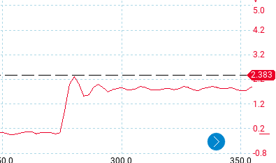
    Upon testing with different combinations, I also saw the overshoot, where the signal went to approximately 2.2 V and then stabilizes at 1.8 V.

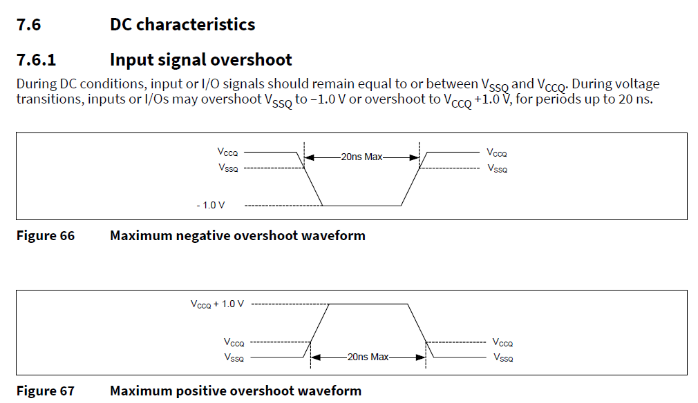
    I discussed this internally, and looks like this is normal as the overshoot is seen for less than 20 ns duration at my setup. The overshoot was seen until 2.2 V which is < Vccq + 1.0 V. Please find the relevant snippet from the flash datasheet.

    So the correct combination which you can use is:

    Frequency = 166 MHz

    Divider = 8

    Dummy Clocks (Read) for Controller and Flash as: 24 and 24(set value of 11 as latency code = 11) respectively. Tests also passed with values 20 and 20(set latency code = 8).

    Regards,

    Vaibhav

  • So the correct combination which you can use is:

    Frequency = 166 MHz

    Divider = 8

    I thought the final solution would be changing capture delay. but your conclusion is reducing the OSPI clock. Why?

  • Explicitly changing read delay value from 1 to 5, will not be feasible for production, as this value/number will vary across board samples.


    Hence, robust solution would be to go ahead with 166 MHz / 8. Please note, if PHY enabled reads are done, then frequency will be 166 MHz itself(bandwidth theory 332 MBps), whereas, the write operation would just take a hit to ~22 MHz(bandwidth theory 44 MBps).

    Currently on AM62x, AM62Px, AM62Dx, and so on we have adopted the divider value of 8 as for 8D-8D-8D there is a limitation of the Controller to have the clock divider value as 8. This is there in the 11.2 release.


    We will have this over for AM64x/AM243x as well.

    I hope this helps.

  • as this value/number will vary across board samples.

    Is it so sensitive even with same PCB/layout?

  • Is it so sensitive even with same PCB/layout?

    Yes this number will vary even with same PCB Layout but the key differentiator here would be PVT, mainly temperature, hence, for a same board with different temperature, this value would change.