AM2632-Q1: The nand memory can't reset successfully

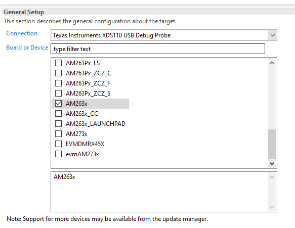
Part Number: AM2632-Q1
Other Parts Discussed in Thread: AM2634, AM2632

Tool/software:

Background:
We are plan to use MT29F4G08ADAFAH4 nand with GPMC. And the program is based on sdk_am263x_10_02_00_13.
There is gpmc_v0 driver module and the file name is gpmc_nandlike_v0.c .The file path is source/drivers/gpmc/v0/
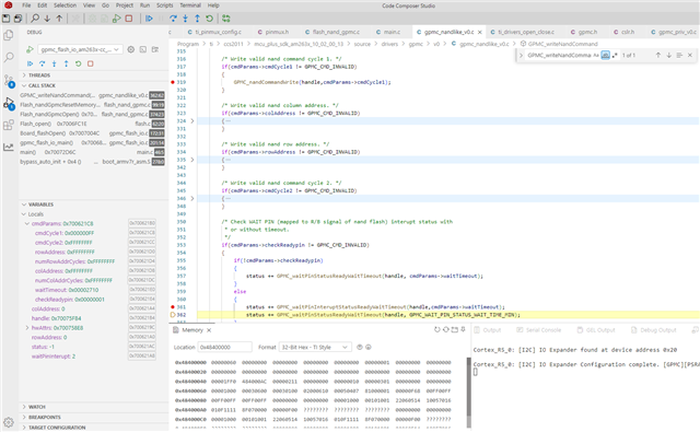
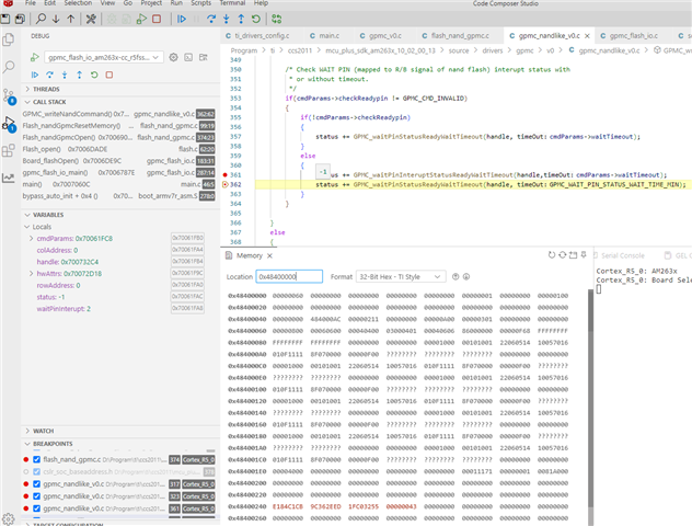
Now we are stuck in the function of GPMC_writeNandCommand() which called by Flash_nandGpmcResetMemory() in flash_nand_gpmc.c

Question
In function GPMC_writeNandCommand(), the GPMC_waitPinInteruptStatusReadyWaitTimeout() always return -1 after calling GPMC_nandCommandWrite(handle,cmdParams->cmdCycle1);
I think that we can't reset memory successfully.


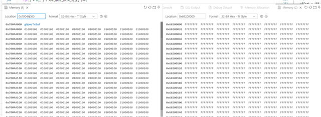
You can see picture for more information.
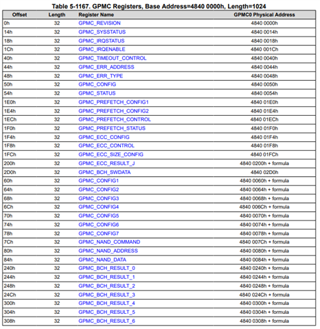
Command Register : 0x4840007C and Address Register : 0x48400080
The cmdParams->cmdCycle1 is 0xFF

  • Hi Wei Yao,

    Firstly, the provided project is not tested on our end as we do not have a board with NAND Flash available as previously communicated. We’ve provided an initial port from AM243x SDK to AM263x to start testing and optimizing it on your end.

    Could you also please confirm if you have a workaround to fix the schematic error of the AD6 and AD7 lines swap? The read/write won’t be successful without that being fixed.

    Thanks and Regards,

    Sahana

  • About AD6 and AD7 lines. I had swapped these two pin offset in ti_pinmux_config.c and tested on these two conditions. It doesn't work.

    On the other hand, we only tested the reset(0xFF) command. So it doesn't matter if these two data lines swap or not.

  • Hi Wei Yao,

    On the other hand, we only tested the reset(0xFF) command. So it doesn't matter if these two data lines swap or not.

    I understand. I was suggesting having a solution to that in order for the rest of the commands to work seamlessly. 

    Do you see the control signals (CS, ADV#/ALE, BE0#/CLE, WE#, and GPMC output clock) toggling when the reset command is set?

    If not, we'll need to vary the following timing parameters in ti_drivers_config.c file to these values and check:

    .csOnTime = 0U,
    .csRdOffTime = 6U,
    .csWrOffTime = 6U,
    .advOnTime = 0U,
    .advRdOffTime = 4U,
    .advWrOffTime = 4U,
    .advAadMuxOnTime = 0U,
    .advAadMuxRdOffTime = 0U,
    .advAadMuxWrOffTime = 0U,
    .weOnTtime = 0U,
    .weOffTime = 3U,
    .oeOnTime = 1U,
    .oeOffTime = 4U,
    .oeAadMuxOnTime = 0U,
    .oeAadMuxOffTime = 0U,
    .pageBurstAccess = 0U,
    .rdAccessTime = 4U,
    .wrAcessTime = 6U,
    .rdCycleTime = 6U,
    .wrCycleTime = 6U,
    .wrDataOnMuxBusTime = 0U,
    .cycle2CycleDelay = 0U,
    .busTurnAroundTime = 0U,
    .cycleDelaySameChipSel = CSL_GPMC_CONFIG6_CYCLE2CYCLESAMECSEN_NOC2CDELAY,
    .cycleDelayDiffChipSel = CSL_GPMC_CONFIG6_CYCLE2CYCLEDIFFCSEN_NOC2CDELAY,

    Could you also provide the dump of all the GPMC registers using CCS register view (Right click and export to text file):


    Regards,

    Sahana

  • 1 Unfortunately, we can't open GPMC and MMC Registers and others can be opened. I don't know the reason. You can see below picture. Also, There is no selection after Right click.

    2 I think we can get register value from Memory view. You can also see below picture. The value is 0x0000,0211 at address 0x48400048. It seems that the error is due to a non supported address. 

    3 About CS Base Address : In am243x demo, the base address is 0x5000,0000. It's a FSS Memory Regions. But There is not same region in am263x. We address is 0x6800,0000 in our project.

    4 About Input Clock Frequency : The frequency is now 0x1000,0000. Is it right? Where can we get the right value. As this value is 1333,3333 in am243x demo. But it can' work when we set 1333,3333 in our am263x project.

  • Another question, Now I don't know how to check the control signals (CS, ADV#/ALE, BE0#/CLE, WE#, and GPMC output clock) toggling when the reset command is set?

  • Hello, Sahana. The reset command return value is ok. Now I test Flash_nandGpmcReadId() fuction.

  • Unfortunately, we can't open GPMC and MMC Registers and others can be opened. I don't know the reason. You can see below picture. Also, There is no selection after Right click.

    You'll need to check for software updates in CCS in order to see this. Click on Help -> Check for updates and perform the updates. You'll then be able to see the registers.  I'll be able to confirm the timing values with the help of these registers.

    About CS Base Address : In am243x demo, the base address is 0x5000,0000. It's a FSS Memory Regions. But There is not same region in am263x. We address is 0x6800,0000 in our project.

    0x68000000 is the right base address for AM263x.

    Frequency is 100MHz in case of AM263x.

    Another question, Now I don't know how to check the control signals (CS, ADV#/ALE, BE0#/CLE, WE#, and GPMC output clock) toggling when the reset command is set?

    I meant to probe these signals on the board to view on a scope.

    Regards,

    Sahana

  • You'll need to check for software updates in CCS in order to see this. Click on Help -> Check for updates and perform the updates. You'll then be able to see the registers.  I'll be able to confirm the timing values with the help of these registers.

    Also ensure to use "AM263x" in the target configuration ccxml file, and not AM2634/AM2632 or any other:

  • Read ID command (0x90) would need to be sent as 0x50 in your case since the AD6/AD7 lines are swapped. have you done this change?

    It is recommended to have a hardware fix for this, else the software development would become complex in-order to interpret the data and command with these data lines swapped.

  • Thank you, The problem has been resolved after sending 0x50 instead of 0x90.

  • Hello Sahana, Now I can write and read nand flash successfully. And read content is consistent with the written content.

    But how can I see the written content in memory? I checked the address 0x6820,0000(base+offset) in debug session and the value is 0xFF.

    You can see below picture. The left is written content in RAM.

  • Hi Wei Yao,

    Are you using the API "GPMC_nandReadData" to perform the read? Also ensure that DMA is not being used to perform the read, as it has not been configured in the project.

    Following is the current configuration in the project, so you would only be able to read 16MB at a time with the start address 0x68000000. You could also modify the chip select size to 128MB to map to the entire GPMC Data size available (0x68000000 - 0x6FFFFFFF) 

  • Hello Sahana, Now the gpmc and nand works fine. And I want to know if we can add DMA function in AM263x.