MSPM0G3519: Transmitting 24 bit SPI frames

Part Number: MSPM0G3519
Other Parts Discussed in Thread: DRV3901-Q1,

Tool/software:

Hello,

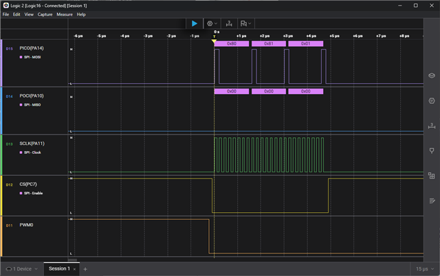
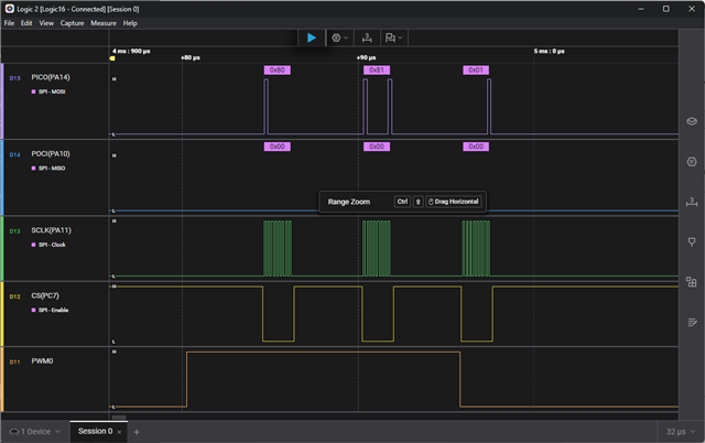
I need to communicate to DRV3901-Q1 devices which require 24 bit frames. What would be the approaches to implement this?

  • Manual CS control
  • or using PACKEN is possible

I would line to use DMA and not sure if manual CS is possible with DMA.

Any suggestion/advice would be helpful.

Regards,

Eugene

  • It's my understanding that PACKEN is non-functional, though I haven't seen an Erratum to that effect [Ref to Refs]

    I recommend using a manual (GPIO) /CS. [Ref] With SPI, /CS can be de-asserted after the Rx-side (DMA) is complete.

    Each FIFO has 4 entries (bytes in your case), so a 3-byte transfer might not benefit much from DMA.

  • Yes. I saw the references to errata on PACKEN. However, MSPM0G351x errata does not list it. Does it work for MSPM0G3519?

    Assuming that PACKEN works, will SPI transmit 24b if I set CTL0.DSS to 8 bits out of two Tx FIFO entries with auto CS control or receive 24b into RX FIFO?

  • I haven't seen such an Erratum for any of the C/L/G series, so I don't know if it has been fixed. The C-series TRM (2 months ago) still describes the feature.

    In one of the threads I mentioned (indirectly), the poster wrote a word with 2x16-bit frames to TXDATA and only one of them appeared on the wire. Even within the (somewhat thin) description of PACKEN, I would say that's non-function.

    The feature does seem to anticipate having an even number of frames to send, which would complicate your case. Maybe 2x12-bit frames would fit.

    I encourage you to actually try this feature before you rely on it in your design.

  • Yes, you are correct. After reading TRM on PACKEN it seems that it is designed to transfer 32 bits to FIFO and no less. 12b idea might work. Will try it. Thanks.

  • With Motorola 4 wire protocol with 8 bit data length , writing three bytes back-to-back into Tx FIFO generates correct CS control for 24 clocks:

    TRM seems to be implying that it is not how it should be.

    Does Motorola 4 wire CS control work around the whole FIFO until it exhausted according to performed number of writes?

  • What SPI mode (particularly CPHA) are you using? TRM Sec 25.2.3.1 distinguishes the /CS behavior based on SPH.

    When I think about writing bytes "continuous back-to-back" I can't help imagining a stray timer interrupt arriving in the middle of the sequence.

  • I can probably achieve back-to-back writes with DMA but that is not the point. I do not see CPHA mentioned in TRM. Are you referring to MSPM0G3519?

    Here is the value of CTL0=0x0000227 which is

    - SPO=0(low)
    - SPH=1(second)
    - CSSEL=0(CS0)
    - CSCLR=0(disable)
    - PACKEN=0
    - FRF=01(Motorola 4 wire)
    - DSS=0111(8 bits)


    It is standard Motorola 4 wire with auto-CS control. Not sure if clock phase control has anything to do with it. The question is the behavior of CS in 4 wire configuration as it is related to TX FIFO. It seems that if there is enough time between writes to TXDATA to shift bits out then CS is toggled around individual bits per DSS. When there is not enough time to shift between writes then all values in TX FIFO are surrounded by CS. See this picture as compared to previous one.

    This is not mentioned anywhere in the TRM and is interesting behavior of the SPI peripheral. One would assume that CS control is around DSS bit count but that is not the case and depends on timing of the writes to TXDATA?

    Is there a configuration I am missing? Would IFLS have anything to do with it?

  • TRM (SLAU846C) Sec 25.2.3.1, in the subsection "Motorola SPI Frame Format with SPO = 0 and SPH = 1" says: "For continuous back-to-back transfers, the CS pin is held low between successive data words". Quoting myself from the thread I referenced above: "based on context and history I interpret [continuous back-to-back] as "the Tx FIFO (+ shift register) never empties"." The SPI unit has no concept of a "transaction" so it has no way of knowing which byte is the final one; instead it "guesses" based on the (Tx) data stream going idle.

    The corresponding paragraph in the subsection "Motorola SPI Frame Format with SPO = 0 and SPH = 0" says: "For continuous back-to-back transmissions, the CS signal must pulse high between each data word transfer because the peripheral-select pin freezes the data in its serial peripheral register and does not allow altering of the data if the SPH bit is clear." This is the distinction based on SPH.

    SPH=CPHA. CPHA is the more common term in the literature. I don't know which term the DRV3901-Q1 documents use, since its datasheet appears to be NDA-only.