AM2432: OSPI RD_DATA_CAPTURE_REG[4:1] DELAY_FLD

Part Number: AM2432

Tool/software:

Hello

I am using a custom board with an AM2432 and a Winbond flash ROM.

1st question:

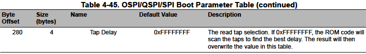
On the TRM, it says that during SPI boot (Primary Boot Mode as SPI), the ROM bootloader automatically selects the appropriate DELAY_FLD value.

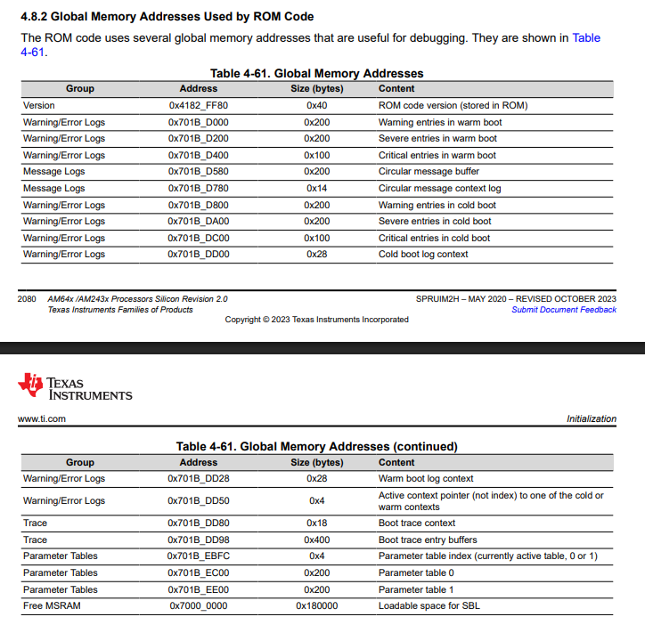
If I need to know the selected result, am I correct to refer to the Boot Parameter Table in the on-chip SRAM? (Address = 0x701BED18, Read data = 0000 in my case)

2nd question:

After the ROM bootloader successfully loads and executes the SBL_OSPI (which was written in the flash), it seems to write a different value to the DELAY_FLD field.

I didn't manage to find the relevant section in the source code of the SBL_OSPI project. Could you point out where?

Again, if I need to know the value of the field, am I correct to refer to the register dump window of CCS? (Expression = OSPI0__OSPI_CFG_VBUSP__VBP2...DELAY_FLD, Read data = 0010 in my case)

I need to know value of the field in order to evaluate the actual waveform, whether it meets the minimum setup and hold time values.

Best regards

  • Hi,

    I would need your help in isolating why you are looking at the address 0x701BED18?

    I found some reference from the TRM:

    2nd question:

    After the ROM bootloader successfully loads and executes the SBL_OSPI (which was written in the flash), it seems to write a different value to the DELAY_FLD field.

    I didn't manage to find the relevant section in the source code of the SBL_OSPI project. Could you point out where?

    Again, if I need to know the value of the field, am I correct to refer to the register dump window of CCS? (Expression = OSPI0__OSPI_CFG_VBUSP__VBP2...DELAY_FLD, Read data = 0010 in my case)

    For this, allow me sometime until I can comment on this and elaborate on how you can interpret these values properly.

    Meanwhile can you help answer the query above.

    Best Regards,

    Vaibhav

  • Thank you for your reply.

    The address 0x701BED18 is part of Parameter Table 0 starting at 0x701BEC00.

    As shown in Table 4-45 "OSPI/QSPI/SPI Boot Parameter Table" of the TRM, byte offset 200 (decimal) seems to retain the "Tap Delay" value selected during boot.

    Table 4-46.

    I referred to this address because the RD_DATA_CAPTURE_REG register seemed to be over-written by the SBL.

    Best regards,

    Daisuke

  • Hi,

    I would recommend reading the value which is 0xFC40010 directly from the memory browser.

    Now, how to know exactly what ROM set as read data capture value.

    Well for this, you would need to stop at the top of your bootloader.

    For example, if my bootloader is SBL NULL, then I put a loop_forever at the beginning of the main.c file as shown below:

    Similarly, if your bootloader is SBL OSPI, then you have to put loop_forever at the topmost line inside main.c.

    Once done, you can flash all the binaries,  then proceed to boot, and this way just after the flow comes out of ROM, it will be stuck at the forever loop.

    Now, you can connect to the R500 core in the CCS IDE.

    Here, you would just need to load symbols, in this case your symbol would look like SBL_OSPI.debug.out file.

    For me it was: C:\ti\mcu_plus_sdk_am64x_11_01_00_17\examples\drivers\boot\sbl_null\am64x-evm\r5fss0-0_nortos\ti-arm-clang\sbl_null.debug.out

    Now you can head over to memory browser and put in 0xFC40010. This way you will get the value from bits[4:1].

    Thanks,

    Vaibhav

  • I didn't manage to find the relevant section in the source code of the SBL_OSPI project. Could you point out where?

    For finding the value being set, after ROM configures the field FC40010 bits[4:1], you would need to look out for the API call which happens as follows:

    Board_driversOpen --> ...... --> Flash_norOspiOpen/Flash_nandOspiOpen --> OSPI_setRdDataCaptureDelay.

    The API OSPI_setRdDataCaptureDelay is responsible for settings the bits[4:1] in 0xFC40010.

    Hopefully this helps you out.

  • I would recommend reading the value which is 0xFC40010 directly from the memory browser.

    Thank you for your prompt reply.

    I feel that I can follow your suggestions and get to the value I want.
    However, is the "Tap Delay" value (byte offset 200) in the parameter table (0x701BEC00) different from the DELAY_FLD value?

  • Hi,

    The value is not different. It is the same one as in Delay_Fld.

    Thanks,

    Vaibhav