Part Number: AM2431
Other Parts Discussed in Thread: SYSCONFIG, UNIFLASH
This is regarding two different items on XIP:
-
Benchmarking
I am trying to do some XIP benchmarking on the EVM AM243x and I am running the example benchmark project that was provided in the SDK. I am seeing higher numbers on SDK 11.02.00.24 vs SDK 10.01.00.32.
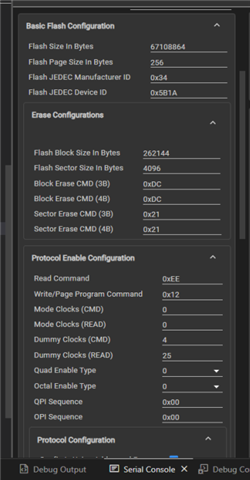
On 10.01-> OSPI input clock was 133.33MHz with a clock divider of 4 with DDR and PHY mode. The FIR filter computation - Max/Flash read execution time matches what is listed in the SDK guide as XIP sample output around ~55000 cycles.
On 11.02 -> OSPI input clock is 166.66MHz with a clock divider of 4 with DDR and PHY mode.
Here the same FIR filter computation - max value is about ~85000 to 87000 cycles when compared to the estimated output at ~58000 to 59000 cycles.
I tried a clock divider value of 2 and the flash initialization in "Board_drivers_open()" failed. I did some digging and came across this thread : https://e2e.ti.com/support/microcontrollers/arm-based-microcontrollers-group/arm-based-microcontrollers/f/arm-based-microcontrollers-forum/1477978/mcu-plus-sdk-am243x-questions-about-ospi-ineffective-8d-mode/5680440?tisearch=e2e-sitesearch&keymatch=AM243x%252525252520OSPI%252525252520speeds#
This is listing a valid configuration for the OSPI controller and the potential configurations to get PHY mode working. Please confirm this is true on SDK 11.02 as well.
As per this thread, when PHY mode is enabled in sysconfig, the clock divider is skipped and uses the input clock as is. https://e2e.ti.com/support/processors-group/processors/f/processors-forum/1431856/faq-am62x-am62ax-am62px-am62d-q1-am64x-am243x-ospi-phy-tuning-algorithm
So with 8D-8D-8D at 166.66MHz, we should be able to achieve ~300MB/s bandwidth.
How to make sure I am actually using the PHY mode and also OSPI is clocking at the right frequency from SW/FW?
What changed in the latest SDK ? Is this performance expected ?
-
Flash write in XIP
Here is my thoughts right now. Please let me know if this is feasible.
- Via sysconfig place the required write function to the flash in a section on SRAM.
- Mark the required flash region with WR permission on the MPU but keep the rest for XIP with RD permission.
- When the interrupt is triggered for flash write, stop/halt my application execution from flash.
- Disable DAC Mode. (May be not required)
- Call the flash write function to perform the desired writes.
Thanks,
Prasanna