This thread has been locked.

If you have a related question, please click the "Ask a related question" button in the top right corner. The newly created question will be automatically linked to this question.

TMS570LC4357-EP: TMS570LC4357 MibSPI DMA Transfer Limit and Large Data (12KB) Transmission Clarification

Part Number: TMS570LC4357-EP
Other Parts Discussed in Thread: HALCOGEN

Hi,

I am working on the TMS570LC4357-EP and trying to use MibSPI with DMA for transmit-only operation.

I referred to the HALCoGen example (example_mibspiDma), where the transfer size is limited to 128 words. I understand that this may be related to the MibSPI RAM / transfer group size.

My requirement is to transmit around 12KB of data continuously using DMA.

I have the following questions:

1. Is the 128-word limit due to MibSPI RAM size per transfer group?
2. What is the correct way to configure DMA for large data transfers like 12KB?
- Should I use frame count to split the transfer into chunks?
3. How exactly should Element Count and Frame Count be configured in this case?
- For example, if using 128-word chunks, is it correct to set:
Element Count = 128
Frame Count = total_words / 128 ?
4. Is there any recommended approach (e.g., ping-pong buffering or transfer group chaining) for efficient large data transmission?
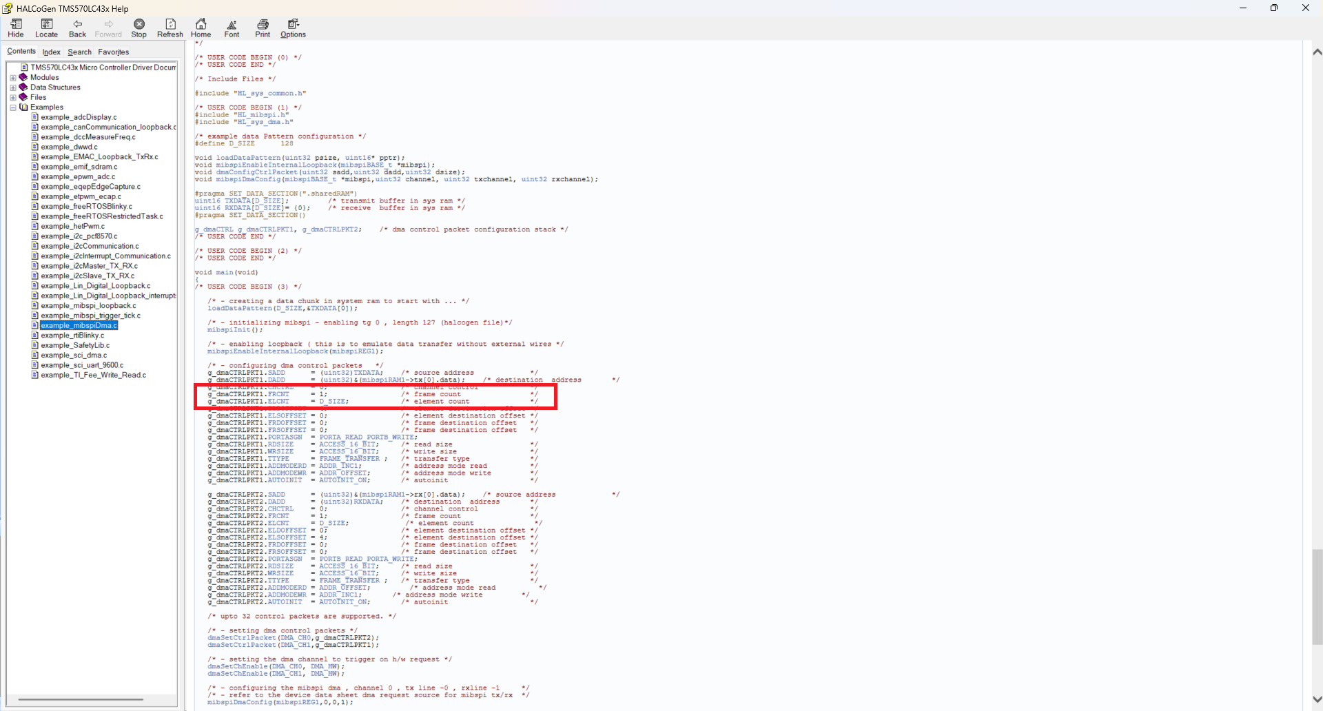
Screenshot 2026-03-19 181340.png
My use case is transmit-only, and I want to minimize CPU intervention.

  • Hi  ,

    Thank you for your previous response. I went through the referenced thread and the technical reference manual, but I still have some confusion regarding large data transfers using DMA on the TMS570LC4357-EP. My requirement is to transmit around 12KB of data using MibSPI with DMA (TX only). I understand that MibSPI has a limited buffer size (e.g., 128 words per transfer group), and the example code also uses 128 elements.

    However, I would prefer not to use DMA channel chaining (i.e., triggering one DMA channel from another), because:
    1. My data size is relatively large (12KB), and
    2. The device has a limited number of DMA channels (32), which I need to reserve for other peripherals as well.

    From the TRM, I see that the DMA supports very large transfer sizes (up to hundreds of MB), so I would like to understand how to configure a single DMA channel to handle this.

    Specifically, I have the following questions:

    1. Is it correct to configure a single DMA channel using Element Count and Frame Count to handle the entire 12KB transfer?

    2. If I configure:
    - Element Count = 128 (to match MibSPI buffer size)
    - Frame Count = (12KB / 128 elements)

    is this the correct way to split the transfer into multiple frames handled automatically by DMA?

    3. In this configuration, will the DMA automatically transfer all frames sequentially without requiring CPU intervention or channel chaining?

    4. Is this the recommended approach for large MibSPI DMA transfers, or is there any limitation or better method I should consider?

    My use case is transmit-only, and I want to keep CPU involvement minimal while efficiently handling large data.

    Any clarification or example configuration would be very helpful.

  • Hi Vasu,

    Apologies for the delayed response.

    I don't have direct example, but you can try below steps.

    DMA Configuration Approch:

    1. Yes, you can configure a single DMA channel to handle the entire 12KB transfer using Element Count and Frame Count.

    2. Your configuration approach is correct:

      • Element Count = 128 (matching MibSPI buffer size)
      • Frame Count = (12KB / 128 elements) = 96 frames (assuming 1 element = 1 byte)
      • If your elements are 16-bit words, you would need 48 frames (12KB / 256 bytes)
    3. Yes, the DMA will automatically transfer all frames sequentially without CPU intervention or channel chaining. This is the key advantage of the frame-based DMA architecture in the TMS570.

    Implementation Details:

    For MibSPI transfers, consider these important points:

    1. Buffer Management: The MibSPI has limited buffer depth. When configuring:

      • Set the DMA transfer trigger to occur when the MibSPI TX buffer reaches a certain level
      • This ensures the DMA keeps the buffer filled but doesn't overflow it
    2. Transfer Mode: Use the Block Transfer Mode with:

      • DESTMODE = 0 (Address is not modified)
      • SRCMODE = 1 (Address is incremented after each transfer)
      • This keeps writing to the same MibSPI data register while incrementing through your source buffer
    3. Interrupt Configuration:

      • Configure FTC (Frame Transfer Complete) interrupt if you need notification when the entire transfer completes
      • This avoids needing to poll the DMA status

    Sample configuration code:

    // Configure DMA channel for MibSPI transfer
    void configureDmaForMibSpi(uint32 *sourceBuffer, uint32 bufferSizeBytes) {
        // Calculate frame count based on element size (assuming 4 bytes per element)
        uint32 elementCount = 128;  // Match MibSPI buffer size
        uint32 frameCount = bufferSizeBytes / (elementCount * 4);
        
        // Configure DMA channel
        dmaSetCtrlPacket(
            DMA_CH_MIBSPI_TX,       // DMA channel for MibSPI TX
            sourceBuffer,           // Source address (your data buffer)
            (uint32*)&mibspiREG1->TDAT[0], // Destination (MibSPI data register)
            elementCount,           // 128 elements per frame
            frameCount,             // Number of frames to transfer
            DMA_SRCINC_1 | DMA_DSTINC_0 | DMA_SIZE_32 | DMA_TTYPE_FRAME
        );
        
        // Enable DMA channel
        dmaReqAssign(DMA_CH_MIBSPI_TX, DMA_REQ_MIBSPI1_TX);
        dmaSetPriority(DMA_CH_MIBSPI_TX, DMA_PRIORITY_HIGH);
        dmaEnableInterrupt(DMA_CH_MIBSPI_TX, DMA_FTC); // Frame Transfer Complete interrupt
        dmaEnable(DMA_CH_MIBSPI_TX);
        
        // Configure MibSPI to trigger DMA when TX buffer is half empty
        mibspiREG1->INT0 |= (1 << 17); // Enable TX DMA request
    }

    --
    Thanks & regards,
    Jagadish.

  • Hi ,Thank you for your response.I tried to configure MibSPI with DMA in multi-buffer mode as per your suggestion, and I have attached my configuration snapshots. However, the DMA transfer is still not working as expected.Could you please review the configuration and let me know if there is any mismatch or if I have missed anything?

  • Hi Vasu,

    Apologies for the delayed response!

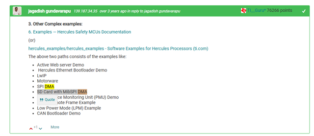
    [FAQ] TMS570LC4357: Examples and Demos for Hercules Controllers (E.g. TMS570x, RM57x and RM46x etc) - Arm-based microcontrollers forum - Arm-based microcontrollers - TI E2E support forums

    Refer below highlighted examples from above link, those are all tested examples from TI side.

    --
    Thanks & regards,
    Jagadish.

  •   

     I have a working solution using software chunking mode that processes the data in 8 separate chunks of 128 words each, and it works perfectly - all 1024 words transfer correctly from TXDATA to RXDATA.However, when I try to use the hardware frame-chain mode to do this more efficiently with a single DMA setup for all 8 frames, I only get the first 128 words transferred. The rest of RXDATA remains as zeros. I've tried various DMA configuration changes but can't get the frame-chain mode to work properly. In frame-chain mode, I set up the DMA for 8 frames of 128 words each, enable the MibSPI DMA events, and let the hardware handle the chaining automatically. But it seems like only the first frame completes successfully, and the subsequent frames don't get processed.Has anyone else encountered this issue with MibSPI frame-chain DMA mode on TMS570LC43? Is there a known limitation or specific configuration required that I'm missing? I've attached my main file. And the second thing is when i tried to download the 1884.LS31x_DMA_Chaining.zip code i got the "You do not have permission to view this directory or page." can you proivde me code might be i got solution( i got this code from the  RM48 SPI2 using DMA ) thread.

    /** @file HL_sys_main.c 
    *   @brief Application main file
    *   @date 11-Dec-2018
    *   @version 04.07.01
    *
    *   This file contains an empty main function,
    *   which can be used for the application.
    */
    
    /* 
    * Copyright (C) 2009-2018 Texas Instruments Incorporated - www.ti.com  
    * 
    * 
    *  Redistribution and use in source and binary forms, with or without 
    *  modification, are permitted provided that the following conditions 
    *  are met:
    *
    *    Redistributions of source code must retain the above copyright 
    *    notice, this list of conditions and the following disclaimer.
    *
    *    Redistributions in binary form must reproduce the above copyright
    *    notice, this list of conditions and the following disclaimer in the 
    *    documentation and/or other materials provided with the   
    *    distribution.
    *
    *    Neither the name of Texas Instruments Incorporated nor the names of
    *    its contributors may be used to endorse or promote products derived
    *    from this software without specific prior written permission.
    *
    *  THIS SOFTWARE IS PROVIDED BY THE COPYRIGHT HOLDERS AND CONTRIBUTORS 
    *  "AS IS" AND ANY EXPRESS OR IMPLIED WARRANTIES, INCLUDING, BUT NOT 
    *  LIMITED TO, THE IMPLIED WARRANTIES OF MERCHANTABILITY AND FITNESS FOR
    *  A PARTICULAR PURPOSE ARE DISCLAIMED. IN NO EVENT SHALL THE COPYRIGHT 
    *  OWNER OR CONTRIBUTORS BE LIABLE FOR ANY DIRECT, INDIRECT, INCIDENTAL, 
    *  SPECIAL, EXEMPLARY, OR CONSEQUENTIAL DAMAGES (INCLUDING, BUT NOT 
    *  LIMITED TO, PROCUREMENT OF SUBSTITUTE GOODS OR SERVICES; LOSS OF USE,
    *  DATA, OR PROFITS; OR BUSINESS INTERRUPTION) HOWEVER CAUSED AND ON ANY
    *  THEORY OF LIABILITY, WHETHER IN CONTRACT, STRICT LIABILITY, OR TORT 
    *  (INCLUDING NEGLIGENCE OR OTHERWISE) ARISING IN ANY WAY OUT OF THE USE 
    *  OF THIS SOFTWARE, EVEN IF ADVISED OF THE POSSIBILITY OF SUCH DAMAGE.
    *
    */
    
    
    /* USER CODE BEGIN (0) */
    /* USER CODE END */
    
    /* Include Files */
    
    #include "HL_sys_common.h"
    
    /* USER CODE BEGIN (1) */
    #include "HL_mibspi.h"
    #include "HL_sys_dma.h"
    #include "HL_sys_core.h"
    #include "HL_reg_esm.h"
    
    #define TG_WORDS 128
    #define D_SIZE TG_WORDS
    #define TOTAL_BYTES 2048
    #define TOTAL_WORDS (TOTAL_BYTES / 2U)
    #define NUM_CHUNKS (TOTAL_WORDS / D_SIZE)
    /* 0 = known-good SW chunk mode, 1 = single HW frame-chain mode */
    #define USE_FRAME_CHAIN 1U


    uint16 tgPSTART1[8]; //for MibSPI1
    g_dmaCTRL g_dmaCTRLPKT_RX, g_dmaCTRLPKT_TX;
    
    #pragma SET_DATA_SECTION(".sharedRAM")
    uint16 TXDATA[TOTAL_WORDS];
    uint16 RXDATA[TOTAL_WORDS] = {0};
    
    #pragma SET_DATA_SECTION()
    
    volatile uint32 transfer512Done = 0U;
    volatile uint32 transfer512Pass = 0U;
    volatile uint32 transfer512FailIndex = 0xFFFFFFFFU;
    volatile uint32 dmaTimeout = 0U;
    
    
    void loadDataPattern(uint32 psize, uint16* pptr, uint16 pattern);
    
    void dmaConfigCtrlRxPacket(uint32 sadd, uint32 dadd, uint16 ElmntCnt, uint16 FrameCnt);
    void dmaConfigCtrlTxPacket(uint32 sadd, uint32 dadd, uint16 ElmntCnt, uint16 FrameCnt);
    /* USER CODE END */
    
    /** @fn void main(void)
    *   @brief Application main function
    *   @note This function is empty by default.
    *
    *   This function is called after startup.
    *   The user can use this function to implement the application.
    */
    
    /* USER CODE BEGIN (2) */
    /* USER CODE END */
    
    int main(void)
    {
    /* USER CODE BEGIN (3) */
    
        uint16 i;
        uint32 tmo;
        uint32 chunk;
        uint32 txAddr;
        uint32 rxAddr;
        uint32 bufid;
    
        esmREG->SR1[0] = 0xFFFFFFFF;
        esmREG->SR1[1] = 0xFFFFFFFF;
        esmREG->SR1[2] = 0xFFFFFFFF;
    
        _enable_IRQ_interrupt_();
    
        mibspiInit();
    
        /* Polling-based DMA test: keep MibSPI TG interrupt disabled to avoid ISR trapping. */
        mibspiDisableGroupNotification(mibspiREG1, 0U);
    
        mibspiEnableLoopback(mibspiREG1, Digital_Lbk);
        mibspiREG1->TICKCNT = (0 << 31) | (0<<28) | (0x100);
    
    
        mibspiREG1->TGCTRL[0U] = (uint32)((uint32)1U << 30U) /* oneshot */
        | (uint32)((uint32)0U << 29U) /* pcurrent reset */
        | (uint32)((uint32)TRG_ALWAYS<< 20U) /* trigger event */
        | (uint32)((uint32)TRG_DISABLED << 16U) /* trigger source */
        | (uint32)((uint32)0U << 8U); /* start buffer */
    
        mibspiREG1->TGCTRL[1U] = (uint32)((uint32)1U << 30U) /* oneshot */
        | (uint32)((uint32)0U << 29U) /* pcurrent reset */
        | (uint32)((uint32)TRG_ALWAYS << 20U) /* trigger event */
        | (uint32)((uint32)TRG_DISABLED << 16U) /* trigger source */
        | (uint32)((uint32)D_SIZE << 8U); /* TG1 start; TG0 size = D_SIZE */
    
    
        /* MibSPI1 TG0 controls: all TG_WORDS use CS0; hold CS until last word. */
        for (i = 0U; i < (D_SIZE - 1U); i++)
        {
            mibspiRAM1->tx[i].control = (uint16)((uint16)5U << 13U) /* buffer mode */
            | (uint16)((uint16)1U << 12U) /* chip select hold */
            | (uint16)((uint16)0U << 10U) /* enable WDELAY */
            | (uint16)((uint16)0U << 11U) /* lock transmission */
            | (uint16)((uint16)0U << 8U)  /* data format */
            | ((uint16)(~((uint16)0xFFU ^ (uint16)CS_0)) & (uint16)0x00FFU); /* chip select */
        }
        mibspiRAM1->tx[D_SIZE - 1U].control = (uint16)((uint16)5U << 13U) /* buffer mode */
        | (uint16)((uint16)0U << 12U) /* chip select hold off for last word */
        | (uint16)((uint16)0U << 10U) /* enable WDELAY */
        | (uint16)((uint16)0U << 8U)  /* data format */
        | ((uint16)(~((uint16)0xFFU ^ (uint16)CS_0)) & (uint16)0x00FFU); /* chip select */
    
    
        tgPSTART1[0] = (mibspiREG1->TGCTRL[0U] >> 8U) & 0xFFU;
    
        dmaEnable();
    
        loadDataPattern(TOTAL_WORDS, &TXDATA[0], 0x7000U);
    #if (USE_FRAME_CHAIN == 1U)
        /* Restore TG0 baseline setup used by software start. */
        mibspiREG1->TGCTRL[0U] = (mibspiREG1->TGCTRL[0U] & 0x9F00FFFFU)
                               | ((uint32)1U << 30U) | ((uint32)0U << 29U)
                               | ((uint32)TRG_ALWAYS << 20U) | ((uint32)TRG_DISABLED << 16U);
    
        /* Frame-chain mode: one DMA packet covers all chunks as frames. */
        dmaConfigCtrlTxPacket((uint32)&TXDATA[0], (uint32)&(mibspiRAM1->tx[tgPSTART1[0]].data), D_SIZE, NUM_CHUNKS);
        dmaConfigCtrlRxPacket((uint32)&(mibspiRAM1->rx[tgPSTART1[0]].data), (uint32)&RXDATA[0], D_SIZE, NUM_CHUNKS);
        dmaSetCtrlPacket(DMA_CH1, g_dmaCTRLPKT_TX);
        dmaSetCtrlPacket(DMA_CH0, g_dmaCTRLPKT_RX);
    
        /* Reset TX/RX RAM address back to TG0 start on each frame. */
        dmaRAMREG->PCP[DMA_CH1].FIOFF = (uint32)(((uint32)((uint16)(0U - (D_SIZE * 4U))) << 16U) | 0U);
        dmaRAMREG->PCP[DMA_CH0].FIOFF = (uint32)((0U << 16U) | (uint32)(uint16)(0U - (D_SIZE * 4U)));
    
        dmaReqAssign(DMA_CH1, DMA_REQ1); /* TX */
        dmaReqAssign(DMA_CH0, DMA_REQ0); /* RX */
    
        /* MibSPI TG0 DMA mapping and large-count setup. */
        bufid = tgPSTART1[0U] + D_SIZE - 1U;
        /* Keep oneshot in this restored state. */
        mibspiREG1->DMACTRL[0U] = 0U;
        mibspiREG1->DMACTRL[0U] |= (1U << 20U) | (0U << 16U); /* rx line1, tx line0 */
        mibspiREG1->DMACTRL[0U] |= 0x8000C000U;               /* enable RX/TX DMA events */
        mibspiREG1->DMACTRL[0U] |= (bufid << 24U);
        mibspiREG1->DMACNTLEN = 1U;
        mibspiREG1->DMACOUNT[0U] = (NUM_CHUNKS - 1U) << 16U;
    
        dmaREG->FTCFLAG = ((uint32)1U << DMA_CH1) | ((uint32)1U << DMA_CH0);
        dmaREG->BTCFLAG = ((uint32)1U << DMA_CH1) | ((uint32)1U << DMA_CH0);
        dmaSetChEnable(DMA_CH1, DMA_HW);
        dmaSetChEnable(DMA_CH0, DMA_HW);
    
        mibspiREG1->TGINTFLG = (mibspiREG1->TGINTFLG & 0x0000FFFFU) | ((uint32)1U << 16U);
        mibspiTransfer(mibspiREG1, 0U);
        tmo = 2000000U;
        while ((dmaGetInterruptStatus(DMA_CH0, BTC) == false) && (tmo > 0U))
        {
            tmo--;
        }
        if (tmo == 0U)
        {
            dmaTimeout = 1U;
        }
    #else
        for (chunk = 0U; chunk < NUM_CHUNKS; chunk++)
        {
            txAddr = (uint32)&TXDATA[chunk * D_SIZE];
            rxAddr = (uint32)&RXDATA[chunk * D_SIZE];
    
            /* 1) DMA TX: source buffer -> MibSPI TX RAM (16 words) */
            dmaConfigCtrlTxPacket(txAddr, (uint32)&(mibspiRAM1->tx[tgPSTART1[0]].data), D_SIZE, 1U);
            dmaSetCtrlPacket(DMA_CH1, g_dmaCTRLPKT_TX);
            dmaREG->FTCFLAG = (uint32)1U << DMA_CH1;
            dmaSetChEnable(DMA_CH1, DMA_SW);
            tmo = 1000000U;
            while ((dmaGetInterruptStatus(DMA_CH1, FTC) == false) && (tmo > 0U))
            {
                tmo--;
            }
            if (tmo == 0U)
            {
                dmaTimeout = 1U;
                break;
            }
    
            /* 2) Run one TG0 SPI transfer */
            mibspiREG1->TGINTFLG = (mibspiREG1->TGINTFLG & 0x0000FFFFU) | ((uint32)1U << 16U);
            mibspiTransfer(mibspiREG1, 0U);
            tmo = 1000000U;
            while ((mibspiIsTransferComplete(mibspiREG1, 0U) == false) && (tmo > 0U))
            {
                tmo--;
            }
            if (tmo == 0U)
            {
                dmaTimeout = 1U;
                break;
            }
    
            /* 3) DMA RX: MibSPI RX RAM -> destination buffer (16 words) */
            dmaConfigCtrlRxPacket((uint32)&(mibspiRAM1->rx[tgPSTART1[0]].data), rxAddr, D_SIZE, 1U);
            dmaSetCtrlPacket(DMA_CH0, g_dmaCTRLPKT_RX);
            dmaREG->FTCFLAG = (uint32)1U << DMA_CH0;
            dmaSetChEnable(DMA_CH0, DMA_SW);
            tmo = 1000000U;
            while ((dmaGetInterruptStatus(DMA_CH0, FTC) == false) && (tmo > 0U))
            {
                tmo--;
            }
            if (tmo == 0U)
            {
                dmaTimeout = 1U;
                break;
            }
        }
    #endif
    
        _dCacheInvalidate_();
    
        transfer512Pass = 1U;
        for (i = 0U; i < TOTAL_WORDS; i++)
        {
            if (RXDATA[i] != TXDATA[i])
            {
                transfer512Pass = 0U;
                transfer512FailIndex = i;
                break;
            }
        }
        transfer512Done = 1U;
    
        while(1)
        {
        }
    /* USER CODE END */
    
        return 0;
    }
    
    
    /* USER CODE BEGIN (4) */
    void loadDataPattern(uint32 psize, uint16* pptr, uint16 pattern)
    {
        int i;
        for(i=0;i<psize;i++)
        {
            *(pptr++) = pattern + i;
        }
    }
    
    
    void dmaConfigCtrlTxPacket(uint32 sadd, uint32 dadd, uint16 ElmntCnt, uint16 FrameCnt)
    {
        g_dmaCTRLPKT_TX.SADD = sadd; /* source address */
        g_dmaCTRLPKT_TX.DADD = dadd; /* destination address */
        g_dmaCTRLPKT_TX.CHCTRL = 0; /* channel control */
        g_dmaCTRLPKT_TX.FRCNT = FrameCnt ; /* frame count */
        g_dmaCTRLPKT_TX.ELCNT = ElmntCnt; /* element count */
        g_dmaCTRLPKT_TX.ELDOFFSET = 4; /* element destination offset */
        g_dmaCTRLPKT_TX.ELSOFFSET = 0; /* element destination offset */
        g_dmaCTRLPKT_TX.FRDOFFSET = 0; /* frame destination offset */
        g_dmaCTRLPKT_TX.FRSOFFSET = 0; /* frame destination offset */
        g_dmaCTRLPKT_TX.PORTASGN = PORTA_READ_PORTB_WRITE; /* port b */
        g_dmaCTRLPKT_TX.RDSIZE = ACCESS_16_BIT; /* read size */
        g_dmaCTRLPKT_TX.WRSIZE = ACCESS_16_BIT; /* write size */
        g_dmaCTRLPKT_TX.TTYPE = FRAME_TRANSFER ; /* transfer type */
        g_dmaCTRLPKT_TX.ADDMODERD = ADDR_INC1; /* address mode read */
        g_dmaCTRLPKT_TX.ADDMODEWR = ADDR_OFFSET; /* address mode write */
        g_dmaCTRLPKT_TX.AUTOINIT = AUTOINIT_OFF; /* autoinit */
    
        //return g_dmaCTRLPKT_TX;
    }
    
    
    void dmaConfigCtrlRxPacket(uint32 sadd, uint32 dadd, uint16 ElmntCnt, uint16 FrameCnt)
    {
        g_dmaCTRLPKT_RX.SADD = sadd; /* source address */
        g_dmaCTRLPKT_RX.DADD = dadd; /* destination address */
        g_dmaCTRLPKT_RX.CHCTRL = 0; /* channel control */
        g_dmaCTRLPKT_RX.FRCNT = FrameCnt; /* frame count */
        g_dmaCTRLPKT_RX.ELCNT = ElmntCnt; /* element count */
        g_dmaCTRLPKT_RX.ELDOFFSET = 0; /* element destination offset */
        g_dmaCTRLPKT_RX.ELSOFFSET = 4; /* element source offset */
        g_dmaCTRLPKT_RX.FRDOFFSET = 0; /* frame destination offset */
        g_dmaCTRLPKT_RX.FRSOFFSET = 0; /* frame source offset */
        g_dmaCTRLPKT_RX.PORTASGN = PORTB_READ_PORTA_WRITE; /* port b */
        g_dmaCTRLPKT_RX.RDSIZE = ACCESS_16_BIT; /* read size */
        g_dmaCTRLPKT_RX.WRSIZE = ACCESS_16_BIT; /* write size */
        g_dmaCTRLPKT_RX.TTYPE = FRAME_TRANSFER ; /* transfer type */
        g_dmaCTRLPKT_RX.ADDMODERD = ADDR_OFFSET; /* address mode read */
        g_dmaCTRLPKT_RX.ADDMODEWR = ADDR_INC1; /* address mode write */
        g_dmaCTRLPKT_RX.AUTOINIT = AUTOINIT_OFF; /* autoinit */
    
        //return g_dmaCTRLPKT_RX;
    }
    /* USER CODE END */
    

  • Hi Vasu,

    Apologies for the delayed response.

    I never did channel DMA chaining for MibSPI channels.

    I did DMA chaining for memory-to-memory transfers and tested; here is the corresponding example:

    2045.DMA_Channel_Chaining_Test_LS3137.zip

    --
    Thanks & regards,
    Jagadish.