This thread has been locked.

If you have a related question, please click the "Ask a related question" button in the top right corner. The newly created question will be automatically linked to this question.

AM2434: GPMC Burst Mode Word Ordering Issue (16‑bit Bus to FPGA, Sync NOR‑like)

Part Number: AM2434
Other Parts Discussed in Thread: AM6442, SYSCONFIG

Hello,

I am experiencing an unexpected word‑ordering issue when using the GPMC in synchronous burst NOR‑like mode with a 16‑bit external data/address bus connected to an FPGA.

When I write a 32‑bit value from the CPU, the two 16‑bit half‑words appear swapped on the external bus, but only when burst mode is enabled.

Example:
*(uint32_t*)0x500000F0 = 0x12345678;
[0x50000000 is the GPMC base address

Observed inside the FPGA using an internal logic analyzer:

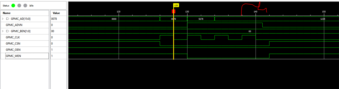
  • Burst mode: the GPMC outputs 0x1234 first, then 0x5678 (upper half‑word first)
  • Non‑burst mode: the FPGA receives 0x5678 first, then 0x1234 (correct order)

This behavior happens only in burst mode.
see picture of without burst:

image.png
see picture of with burst:
image.png

How can I control or correct the half‑word ordering when using GPMC burst write mode?

My GPMC configuration with burst enabled:
GPMC_CONFIG1 = 939528704 
GPMC_CONFIG2 = 132352 
GPMC_CONFIG3 = 65792 
GPMC_CONFIG4 = 33645841 
GPMC_CONFIG5 = 17105413 
GPMC_CONFIG6 = 2164326400

My configuration without burst (which works as expected):
GPMC_CONFIG1 = 671093248
GPMC_CONFIG2 = 132352
GPMC_CONFIG3 = 65792
GPMC_CONFIG4 = 33645841
GPMC_CONFIG5 = 17105413
GPMC_CONFIG6 = 2164326400

Additional details:

  • External device: FPGA
  • Bus width: 16‑bit
  • Mode: synchronous burst NOR‑like
  • Data captured inside FPGA (internal logic analyzer)

Any guidance on how to fix or configure the correct half‑word order during GPMC burst writes would be appreciated.

  • Hi Ariel,

    Thank you for your query !

    Please allow me some time to internally discuss with the topic owner.

    I may need to reach out to our GPMC HW and SW experts.

    I hope I can get back to you with a response by Monday (March-30-2026) COB.

    We appreciate your patience !

    Best Regards 

    Anastas Yordanov

  • Hello Ariel,

    Did you try with memcpy like Anil is suggesting in this e2e thread?


    Part Number: AM6442 Hi, I have received a couple general questions from a customer regarding writing code for their AM6442's GPMC peripheral. According to them, they are currently using GPMC in burst…
    By in Processors > Processors forum
    3 replies
     

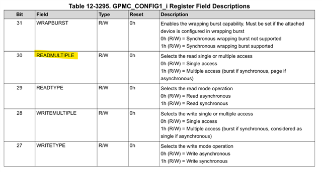
    Also, is it possible for your setup to read back the written  to FPGA data, just for the test? I can see you are not setting the Read Multiple bit, you may need to set it to 1 so we make sure reads and writes are in the same mode:

    I've reached out to GPMC expert, I don't know GPMC internal function and software that good.

    Thanks,

    Stan

  • Hi Stan,

    Thank you much for jumping in !

    Hello Ariel,

    I would like to apologize for the big time gap in my response.

    In order to be able to isolate any possible root cause from software side, can you specify:

    the type (Linux / MCU PLUS) and version of the AM243x SDK you are using ?

    Thanks

    Best Regards

    Anastas Yordanov

  • Hi Stan and Anastas,

    When I read the register after writing, I get the reversed order (which matches the behavior observed in this issue).
    The memcpy operation generates the same data order.

    I also tried configuring the read operation as burst, but this did not resolve the ordering problem.

    Environment:

    • SDK: ind_comms_sdk_am243x_11_00_00_13
    • SysConfig: sysconfig_1.25.0
    • OS: FreeRTOS
    • Active Cores: R5F_0_0, R5F_0_1

    I do not think this is a software issue, because changing the configuration changes the behavior.

    If I change WRACCESSTIME to 2, the configuration becomes:

    GPMC_CONFIG1 = 939528704
    GPMC_CONFIG2 = 132352
    GPMC_CONFIG3 = 65792
    GPMC_CONFIG4 = 33645841
    GPMC_CONFIG5 = 17105413
    GPMC_CONFIG6 = 2181103616

    With this configuration:

    • The data order becomes correct
    • However, I get an extra clock cycle, which also generates a write to an address that I did not request (see picture below)

    Additionally, this configuration fixes the ADVN operation.
    In the original configuration, this line does not work properly.

    I can work with the extra clock cycle if the GPMC requires it. However, in that case, I need WEN or CSN to go to '1' during this cycle, or BEN to go to "11", in order to avoid generating an extra write.

    My main goal is to achieve:

    • 1 clock cycle for the address
    • 1 clock cycle for each data write

    Best Regards

    Ariel Gershengold

  • Hi Ariel,

    My main goal is to achieve:

    • 1 clock cycle for the address
    • 1 clock cycle for each data write

    Is it an option for you to divide down the external clock? This way the controller will have more time to perform internal operations as it still being clocked at internal frequency

     :

  • Hi Stanislav,
    No, we need to work at 100 MHz; otherwise, we will have problems with the time required to transfer the data.

    If we divide the time by 2, it will be the same as working at 100 MHz without burst.

    B.R.
    Ariel Gershengold

  • I can work with the extra clock cycle if the GPMC requires it. However, in that case, I need WEN or CSN to go to '1' during this cycle, or BEN to go to "11", in order to avoid generating an extra write.

    Actually isn't it fixing the double writing at the end of burst? Shortening WEN, CSN times? Did you already try it? Looks to me it would also meet the 1-clock criteria?

    Regards,

    Stan

  • No you can see in the record the BEn is "00" in the double writing. I try to change the WEn and CSn times but I did not see the expected effect. 
    B.R.
    Ariel

  • Hello Ariel

    Thank you for the inputs.

    The expert is out of office on Monday.
    Please expect delay in response.

    Regards,

    Sreenivasa