This thread has been locked.

If you have a related question, please click the "Ask a related question" button in the top right corner. The newly created question will be automatically linked to this question.

AM620-Q1: [VALEO] [AM625-Q1] [SDK V.10]: Implementation to Auto detect NAND Flash chip using ECh command

Part Number: AM625-Q1
Other Parts Discussed in Thread: AM623, , AM620-Q1

Hello TI Support Team,

As you may be aware, there are recent supply chain shortages from NAND Flash memory suppliers.
As a consequence, our projects now require the flexibility to support multiple NAND Flash variants using the same software without recompiling static binaries for each chip.

Our current version of the SDK (sdk 10.00.00 ) is pre-built with static configurations and can not fulfil our current need. So first of all, we want to ask if there is a newer version of the sdk that can fulfill this feature.
Regarding our current SDK, we may need a patch to enable this feature. We are proposing a design that we want to discuss with you to detect the connected NAND chip at runtime using the ONFI Read Parameter Page (ECh) command.

Our Proposed Design Flow:

  1. Initialize the NAND with conservative default configurations.

  2. Issue a RESET (FFh) command as the first operation because it is required by some vendor constraints.

  3. Issue the Read Parameter Page (ECh) command with a 00h address cycle.

  4. Parse a 256-byte paramaters copy and map its data to re-configure the NAND attributes at runtime based on these results.

  5. Write the registers with the true configurations.

  6. Use NAND normally as Read/Write commands.
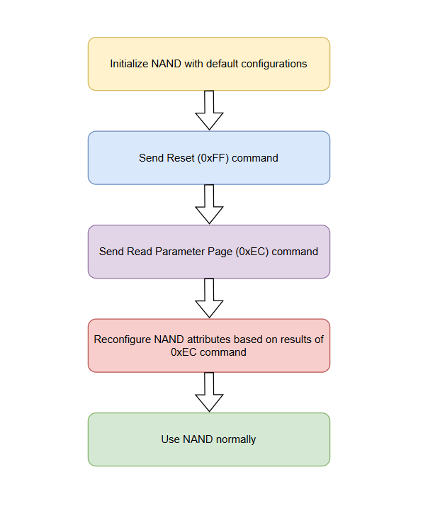
Design_Flowchart.png
We have some questions that we need your kind support to answer:
  1. ROM Code Support: Does the current ROM code for our SoC has a built-in mechanism for "NAND Auto-detection" during the initial boot phase?
    If Yes, Is it based on a similar design as we propose or is there a better approach?
    If No, What is your suggestion on this topic ? as it will be a blocker for us.
      
  2. Proposed design: Do you see a flaw in the proposed design idea?
    Is it safe to start the NAND with default configurations and then re-configure it at run-time? If yes, what can the default configurations be? especially the timing parameters.

  3. GPMC Timing Parameters: We have observed the .timingParams struct in the gGpmcAttrs[] array within ti_drivers_config.c. Will these parameters (e.g., csRdOffTimerdAccessTimeweOnTime) require unique values for each NAND chip used? 
    If the timings must change, what is the official TI recommended mapping between standard NAND timing characteristics mentioned in datasheets and the specific GPMC variables in the configuration array generated from syscfg tool? 

  4. ECh command: what is the correct implementation sequence for ECh command?
    As a proof of concept we tried two sequences but both gave the same incorrect result (command return SUCCESS but data is wrong)

         The 1st trial sequence:
         - Send ECh command with Column address 0x00 and params.checkReadypin = FALSE
         - Send Read Status command 70h
         - Send Read Mode command 00h to enable data output mode
         - Use API GPMC_nandReadData() to fetch the data 

         2nd trial sequence:
         - Send  ECh command with Column address 0x00 and params.checkReadypin = FALSE
         - Wait for a delay (more than Read Page time)
         - Use API GPMC_nandReadData() to fetch the data directly

We look forward to your guidance on whether this dynamic approach can be compatible with the GPMC driver architecture and boot sequence, and in providing an example for the code if the patch is needed.

Thanks in Advance,

  • Hello Reem Abo el Khair,

    Thank you for your query !

    Please allow us some time to discuss over questions from the list internally.

    We may need to involve our ROM and software GPMC driver experts to assess the ROM / SBL software flexibility

    to adapt different NAND flashes to AM623 (teaching their parameters via the 0xEC command).

    Q: Would you please specify the SDK type - is it a LINUX or SDK-MCU-PLUS (RTOSes, Bare-metal)

    Please expect that some delay is possible in our response because of Easter holidays in the US. 


    Thanks

    Best Regards

    Anastas Yordanov

  • Hello Anastas,

    It is SDK-MCU (version 10.00.00) for target AM625-Q1.

    Best Reagrds

  • Hi Reem Abo el khair,

    Thank you for updating us.

    I have conveyed to the AM620-Q1 GPMC hardware and the ROM / SDK MCU + software experts. Still waiting for their reply.

    I will let you know as soon as their reply is available.

    Best Regards,

    Anastas Yordanov

  • Hello,
    Again sorry for the inconvenience but the target as I said in the last reply is AM625-Q1 not AM620-Q1 (I can not edit it in the ticket)


    Also, Here is a snippet of the code that is NOT working, if you can help in identifying the problem:

    uint8_t ParameterPage[768]= {0x0};

    static int32_t Flash_nandReadParameterPage(Flash_Config *config)
    {
        int32_t status = SystemP_SUCCESS;
        Flash_NandGpmcObject *object = NULL;
        Flash_DevConfig *devConfig = NULL;
        GPMC_nandCmdParams params;
        GPMC_Transaction trans;

        /* Input parameter validation. */
        if (config != NULL)
        {
            object = (Flash_NandGpmcObject *)config->object;
            devConfig = (Flash_DevConfig *)config->devConfig;
        }
        else
        {
            status = SystemP_FAILURE;
        }

        if(status == SystemP_SUCCESS)
        {
            /* Prepare command parameters to send Read Parameter Page command. */
            GPMC_writeNandCommandParamsInit(&params);
            params.cmdCycle1 = devConfig->cmdReadParameterPage;
            params.numColAddrCycles  = 1;
            params.colAddress = 0x00;
            params.waitTimeout = NAND_DEVICE_BUSY_TIMEOUT;
            params.checkReadypin = FALSE;

            status += GPMC_writeNandCommand(object->gpmcHandle, &params);
        }


        if(status == SystemP_SUCCESS)
        {
            ClockP_usleep(250000U); /*Safe Delay*/
            GPMC_transactionInit(&trans);
            trans.Buf = ParameterPage;
            trans.count = 768;
            trans.transType = GPMC_TRANSACTION_TYPE_READ;
            /* Read DATA either using the DMA or CPU prefetch read.*/
            status += GPMC_nandReadData(object->gpmcHandle, &trans);
        }

        return status;
    }


    where the timing configurations for GPMC is found here:

    static GPMC_HwAttrs gGpmcAttrs[CONFIG_GPMC_NUM_INSTANCES] =
    {
        {
            .gpmcBaseAddr         = CSL_GPMC0_CFG_BASE,
            .dataBaseAddr         = CSL_GPMC0_DATA_BASE,
            .elmBaseAddr          = CSL_ELM0_BASE,
            .inputClkFreq         = 133333333U,
            .intrNum              = 103U,
            .intrPriority         = 4U,
            .chipSelBaseAddr      = 0x50000000U,
            .chipSelAddrSize      = GPMC_CS_MASK_ADDR_SIZE_16MB,
            .clkDivider           = CSL_GPMC_CONFIG1_GPMCFCLKDIVIDER_DIVBY1,
            .waitPinNum           = CSL_GPMC_CONFIG1_WAITPINSELECT_W0,
            .addrDataMux          = CSL_GPMC_CONFIG1_MUXADDDATA_NONMUX,
            .timeLatency          = CSL_GPMC_CONFIG1_TIMEPARAGRANULARITY_X1,
            .waitPinPol           = CSL_GPMC_CONFIG_WAIT0PINPOLARITY_W0ACTIVEL,
            .timingParams         =
            {
                .csOnTime               =   0U,
                .csRdOffTime            =   5U,
                .csWrOffTime            =   6U,
                .advOnTime              =   0U,
                .advRdOffTime           =   4U,
                .advWrOffTime           =   4U,
                .advAadMuxOnTime        =   0U,
                .advAadMuxRdOffTime     =   0U,
                .advAadMuxWrOffTime     =   0U,
                .weOnTtime              =   0U,
                .weOffTime              =   3U,
                .oeOnTime               =   1U,
                .oeOffTime              =   4U,
                .oeAadMuxOnTime         =   0U,
                .oeAadMuxOffTime        =   0U,
                .pageBurstAccess        =   0U,
                .rdAccessTime           =   5U,
                .wrAcessTime            =   6U,
                .rdCycleTime            =   5U,
                .wrCycleTime            =   5U,
                .wrDataOnMuxBusTime     =   0U,
                .cycle2CycleDelay       =   0U,
                .busTurnAroundTime      =   0U,
                .cycleDelaySameChipSel  =   CSL_GPMC_CONFIG6_CYCLE2CYCLESAMECSEN_NOC2CDELAY,
                .cycleDelayDiffChipSel  =   CSL_GPMC_CONFIG6_CYCLE2CYCLEDIFFCSEN_NOC2CDELAY,
            },
            .eccAlgo                =   GPMC_NAND_ECC_ALGO_BCH_8BIT,
            .readType               =   CSL_GPMC_CONFIG1_READTYPE_RDASYNC,
            .csExDelay              =   CSL_GPMC_CONFIG2_CSEXTRADELAY_NOTDELAYED,
            .accessType             =   CSL_GPMC_CONFIG1_READMULTIPLE_RDSINGLE,
            .optimisedAccess        =   CSL_GPMC_PREFETCH_CONFIG1_ENABLEOPTIMIZEDACCESS_OPTDISABLED,
            .dmaRestrictedRegions   =   gGpmcDmaRestrictRegions,
        },
    };


    We are currently blocked on this topic and we will be grateful for your quick support.

    Best Regards,


  • Hello Reem Abo el khair,

    I'm adding software support to check your code to interrogate parameter page.

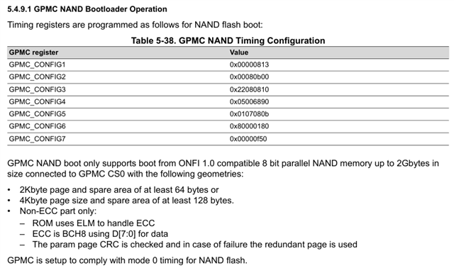
    Regarding ROM, ROM on AM62x does not extract timings from the parameter page on NAND flash. It is rigid with the NAND that are supported and that is documented in TRM 5.4.9.1 GPMC NAND Bootloader Operation (copied below).

    The last line in TRM 5.4.9.1, “GPMC is setup to comply with mode 0 timing for NAND flash”, refers to the attached ONFI spec - Table 12 Timing Modes 0, 1, and 2. Refer to https://onfi.org/files/onfi_1_0_gold.pdf

    The registers provided in TRM Table 5-38 try to match these ONFI mode 0 timings.

    These slow timings are intended to support all ONFI 1.0 compliant NAND flash devices without interrogating their timings.

    The ROM also has restrictions on bus width (8-bit only), density (upto 2Bytes), page size (2K, 4K only), ECC (ECC internal to FLASH not allowed), ECC (BCH8 required).

    Regards,
    Mark

  • Hi,

    I see you are talking about GPMC NAND and not Serial NAND Flash, hence I am reassigning this ticket to the correct expert.

    Regards,

    Vaibhav

  • Hello  Reem Abo el khair,

    I have looked at the code, and it seems to be correct.

    You are sending the EC followed by 0x00, which is correct.

    After issuing the read command for 768 bytes, you are waiting 0.2 seconds before reading the data.

    My suggestion is to set the WaitReady pin to true instead of using a delay, and check whether the status is ready before reading the data.

    In your test case, what exactly happens after issuing the read command? Are all 768 bytes corrupted, or are the first 256 bytes correct?

    Can you please explain the issue you are facing?

    NAND device timing parameters may change based on the operating voltage. We tuned these timing parameters for your NAND device at 1.8V.

    Which NAND device are you currently using? What is the operating voltage? Can you please share the datasheet as well?

    Regards,

    Anil.

  • Hello  Reem Abo el khair,

    Can you also please confirm what is the devConfig->cmdReadParameterPage is used in your application ?

    Regards,

    Anil.

  • Hello,

    The code worked and we were able to read the Parameter page.

    However, we still have questions about the GPMC timing configurations.

    1-Will the timing configurations ( section .timingParams in array static GPMC_HwAttrs gGpmcAttrs[CONFIG_GPMC_NUM_INSTANCES]) differ if we are using a different NAND chip than our current one ?


    2-If yes, what shall be the default value for the .timingParams in the array GPMC_HwAttrs gGpmcAttrs?

    3-How can we do the mapping between the timing specifications values in the datasheet and the 
    GPMC_timingParams struct elements?

    4-Does the current implementation of the MCU SDK use the ONFI timing modes feature ? What is the timing mode that we working with?

    5-For the UBoot, does the firmware speeds up the timings (switches to a higher timing mode) after identifying the NAND chip using the ECh command? Or does it stay in timing mode 0 till the end of flashing?

    Thanks in advance,

  • Hello  Reem Abo el khair,

    The MCU SDK's GPMC requires timing parameters that are tailored to specific NAND devices and operating conditions. These parameters are not universal because each NAND manufacturer has different electrical characteristics. Operating voltage also significantly affects timing. Higher voltage allows faster access, while lower voltage requires slower, more conservative timing.

    We have shared the timing parameters for your NAND device operating at 1.8V.

    If we implement generic NAND timing parameter support for almost all devices, you will experience performance degradation similar to what you already faced. At that time, we optimized the timing parameters specifically for your device.

    We follow an Excel sheet approach. You can provide all timing details from the datasheet, and based on this information, you can choose the appropriate timing parameters.

    /cfs-file/__key/communityserver-discussions-components-files/908/GPMC_2B00_tool.xlsm

    The current MCU SDK does not implement ONFI mode. The SDK does not send mode-switching commands to change NAND timing behavior. The GPMC timing parameters are configured once during GPMC initialization and remain fixed throughout operation.

    This approach is acceptable because the fixed timing parameters are configured to work with the NAND device mounted on the EVM.

    Every NAND read operation follows proper timing sequences (Even ONFI command ). Commands are sent according to the configured timing parameters. Data transfers respect access time and cycle time specifications with the existing timing values.

    For the UBoot, does the firmware speeds up the timings (switches to a higher timing mode) after identifying the NAND chip using the ECh command? Or does it stay in timing mode 0 till the end of flashing?

    I am routing your query to Linux expert for the above comment .

    Regards,

    Anil.

  • Hello Anel,

    In your attached excel sheet I see tab "Reg Dump" in which there is a drop down menu for "GPMC Chip Select" numbered from 0 to 6. Can you please clarify the mapping of each number from them? Do they represent different ECU targets or different NAND Chips ?

    Also, If the different NAND chips I want to support all have the same operating voltage of 1.8V, will I still need different GMPC timing configurations for each one of them ?

    Best Regards,

  • Hello Reem Abo el khair,

    Let me add the nand device configurations in u-boot/kernel in Linux SDK.
    1/. The nand device parameters (i.e. timing, bus width, and chip select...) are configured in GPMC_CONFIGx registers (x=1 to 7)

    2/. GPMC_CONFIGx registers configurations in onchip ROM
    Refer to the note in Mark's early reply.

    3/. GPMC_CONFIGx registers configurations in SPL/u-boot/kernel
    The gpmc-nand device tree node is called through the Driver Model (DM) framework to configure the GPMC_CONFIGx registers. This occurs during the driver probing process, typically initiated when a sub-device (like NAND flash) is accessed. Refer to the two example dtsi/dtso files used in u-boot for your reference.
    https://git.ti.com/cgit/ti-u-boot/ti-u-boot/tree/dts/upstream/src/arm64/ti/k3-am62-main.dtsi?h=12.00.00.07#n1274
    https://git.ti.com/cgit/ti-u-boot/ti-u-boot/tree/dts/upstream/src/arm64/ti/k3-am62-lp-sk-nand.dtso?h=12.00.00.07#n42

    4/. ONFI parameters are read in SPL/u-boot/kernel stages, where only the nand device geometry (i.e. page size, OOB size etc...) are used, but not the nand device timing parameters (which are configured via dtsi/dts/dtso etc...)

    One option for your to consider in Linux SDK:
    - binding the board DT node with the gpmc-nand device, and configuring the DT node for the specific gpmc-nand device
    - dynamially loading DT node or DT overlay based on the board detection

    Best,
    -Hong

  • Hello  Reem Abo el khair,

    You need to check the NAND Timings tab.

    In this tab, you need to enter the memory timing details in column E from the datasheet.

    Based on this information, you need to adjust the timing values in column B. Make sure that while changing these values, the minimum and maximum values remain within the specified range.

    Regards,

    Anil.