Part Number: AM2634
Other Parts Discussed in Thread: DAC81408, , SYSCONFIG
Hi Team,
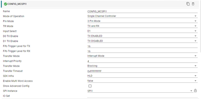
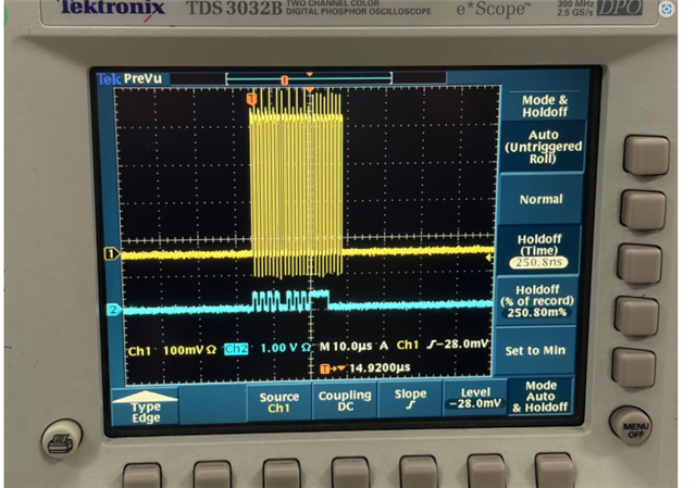
I am currently working on interfacing the DAC81408 module with the AM2634 controller board using the SPI1 interface, but I am unable to observe any output from the DAC.
The connections made are as follows:
- SPI1_D0 → J8 (Pin 3)
- SPI1_D1 → J8 (Pin 4)
- SPI1_CLK → J8 (Pin 8)
- SPI1_CS → J8 (Pin 2)
Additional details:
- Common ground is established between the DAC module and the controller board.
- Proper supply voltages (VCC and VSS) have been applied.
- The reference voltage has been verified, and I am measuring 2.5V at J1 (Pin 7).
Despite these checks, I am still not able to get any output from the DAC. I have attached my code for your reference.
This issue is currently blocking my project progress, so I would greatly appreciate your help at the earliest. Could you please advise if there are any specific SysConfig settings, SPI configurations, or initialization steps required for proper communication?
CODE:
#include <kernel/dpl/ClockP.h>
#include <kernel/dpl/DebugP.h>
#include "ti_drivers_config.h"
#include "ti_drivers_open_close.h"
#include "ti_board_open_close.h"
#include <drivers/hw_include/tistdtypes.h>
#include <stdlib.h>
#include <string.h>
#include "analog_dac.h"
uint32_t startTimeInUSec, elapsedTimeInUsecs;
void *dac81408_main(void *args)
{
Drivers_open();
Board_driversOpen();
Reset_Signal();
startTimeInUSec = ClockP_getTimeUsec();
init_dac81408();
elapsedTimeInUsecs = ClockP_getTimeUsec() - startTimeInUSec;
DebugP_log(" \tTotal Time for Completion : \t\t%5.2f\r\n",(Float32)(elapsedTimeInUsecs / 1));
Board_driversClose();
Drivers_close();
return NULL;
}
/******************************** DAC *********************************************************/
void init_dac81408()
{
DebugP_log(" [SPI1] DAC PINS [DAC0-DAC3] DIFFERENTIAL and SINGLE ENDED[DAC4-DAC7]\r\n");
clear_DAC_Register();
ClockP_usleep(25);
DebugP_log("init_dac81408!!\r\n");
//Setting DAC Register
DAC81408_Settings();
//Setting DAC Range Register
Set_DAC_Range();
//getDAC81408_Status();
//Setting Input Voltage to DAC Out Register
float inVol = 18.6;
DebugP_log("Input Voltage : %f\r\n",inVol);
Set_InputVoltage_To_DAC(inVol);
//getDAC81408_Status();
DebugP_log("exit_dac81408!!\r\n");
}
void SPI_Write_To_DAC(uint8_t reg,uint16_t wdata)
{
MCSPI_Handle spiHandle = NULL;
uint8_t lsb = ((uint16_t)wdata >> 0) & 0xFF;
uint8_t msb = ((uint16_t)wdata >> 8) & 0xFF;
uint8_t txbuffer[3] = {reg,msb,lsb};
SPI_Transaction(spiHandle, txbuffer, sizeof(txbuffer), NULL, 0);
}
void SPI_Read_Frm_DAC(uint8_t reg)
{
MCSPI_Handle spiHandle = NULL;
uint8_t txbuffer[3];
txbuffer[0] = 0x80+reg;//Mask for Data Read from Register
txbuffer[1] = 0x00;
txbuffer[2] = 0x00;
uint8_t rbuffer[3] = {0,0,0};
SPI_Transaction(spiHandle, txbuffer, sizeof(txbuffer), NULL, 0);
ClockP_usleep(5);
SPI_Transaction(spiHandle, NULL , 0, rbuffer, sizeof(rbuffer));
ClockP_usleep(5);
uint16_t res = ((rbuffer[1] << 8) | rbuffer[2]) % 0x10000;
getRegName(reg);
DebugP_log("[SPI_Read_Frm_DAC] res = 0x%04x \r\n", res);
//return res;
}
void SPI_Transaction(MCSPI_Handle spiHandle, uint8_t *txbuffer, size_t txSize, uint8_t *rxbuffer, size_t rxSize)
{
MCSPI_OpenParams openParams;
MCSPI_Transaction spiTransaction;
int32_t transferOK;
MCSPI_OpenParams_init(&openParams);
//spiHandle = MCSPI_open(CONFIG_MCSPI0, &openParams);
spiHandle = MCSPI_open(CONFIG_MCSPI1, &openParams);
//spiHandle = MCSPI_open(CONFIG_MCSPI2, &openParams);
if (spiHandle == NULL)
{
DebugP_log("Error: Unable to open SPI handle.\r\n");
return;
}
SPI_CS_High_Low(0);
MCSPI_Transaction_init(&spiTransaction);
spiTransaction.csDisable = FALSE;
spiTransaction.count = txSize+rxSize;
spiTransaction.txBuf = txbuffer;
spiTransaction.rxBuf = rxbuffer;
transferOK = MCSPI_transfer(spiHandle, &spiTransaction);
if (transferOK != SystemP_SUCCESS)
{
DebugP_log("Error: SPI transfer failed.\r\n");
}
SPI_CS_High_Low(1);
MCSPI_close(spiHandle);
}
/*
* this fun is going to clear the DAC Output Register Value
*
* */
void clear_DAC_Register(void)
{
//CLR PIN in DAC is PIN9 and AM2634 Controller:GPIOPIN 44 and HSEC PIN:51
uint32_t gpioClrDACOutRegBaseAddr = (uint32_t) AddrTranslateP_getLocalAddr(GPIO_CLR_BASE_ADDR);
uint32_t clrDACOutPinNum = GPIO_CLR_PIN;
GPIO_setDirMode(gpioClrDACOutRegBaseAddr, clrDACOutPinNum, GPIO_CLR_DIR);
GPIO_pinWriteLow(gpioClrDACOutRegBaseAddr, clrDACOutPinNum);
ClockP_usleep(25); //As per Data sheet Min delay is 20ns but given max delay for synchronization
GPIO_pinWriteHigh(gpioClrDACOutRegBaseAddr, clrDACOutPinNum);
ClockP_usleep(25);
}
uint16_t CodeVal_UnipolarVoltage_FSR40(float vout)
{
/*
* Vout = ((code/2^n) * FSR)+ Vmin ; As per data sheet
* code = (Vout*2^n)/FSR
*
* FSR : Full Scale Range: (Vmax-Vmin)
* Code : Binary value feed to DACnDATA Register
* Vout : Output Voltage
* 2^n : Resolution : DAC81408 is 16Bit then 2^16 = 65536
*
* NOTE : FSR is Fixed : Single Ended = 0V to 30V
* : Differential : -15V to +15V
* FSR : 0V to 40V Fixed.
* */
uint16_t code = 0;
code = ((vout*RESOLUTION)/FSR_40);
DebugP_log("Single Ended Code Value : %d and 0x%x \r\n",code,code);
return code;
}
uint16_t CodeVal_UnipolarVoltage_FSR20(float vout)
{
uint16_t code = 0;
code = ((vout*RESOLUTION)/FSR_20);
DebugP_log("Single Ended Code Value : %d and 0x%x \r\n",code,code);
return code;
}
uint16_t CodeVal_UnipolarVoltage_FSR10(float vout)
{
uint16_t code = 0;
code = ((vout*RESOLUTION)/FSR_10);
DebugP_log("Single Ended Code Value : %d and 0x%x \r\n",code,code);
return code;
}
uint16_t CodeVal_UnipolarVoltage_FSR5(float vout)
{
uint16_t code = 0;
code = ((vout*RESOLUTION)/FSR_5);
DebugP_log("Single Ended Code Value : %d and 0x%x \r\n",code,code);
return code;
}
int16_t CodeVal_BipolarVoltage(float vout)
{
//DebugP_log("vout = %f \r\n", vout);
int16_t code = 0;
// the range from -10V to +10V and 0 to 65535
code = (uint16_t)((((vout + (FSR_20 / 2)) * RESOLUTION) / FSR_20));
DebugP_log("Differential Code Value : %d and 0x%x \r\n", code, code);
return code;
}
int16_t CodeVal_BipolarVoltage_FSR40(float vout)
{
//DebugP_log("vout = %f \r\n", vout);
int16_t code = 0;
// the range from -10V to +10V and 0 to 65535
code = (uint16_t)((((vout + (FSR_40 / 2)) * RESOLUTION) / FSR_40));
DebugP_log("Differential Code Value : %d and 0x%x \r\n", code, code);
return code;
}
int16_t CodeVal_BipolarVoltage_FSR20(float vout)
{
//DebugP_log("vout = %f \r\n", vout);
int16_t code = 0;
// the range from -10V to +10V and 0 to 65535
code = (uint16_t)((((vout + (FSR_20 / 2)) * RESOLUTION) / FSR_20));
DebugP_log("Differential Code Value : %d and 0x%x \r\n", code, code);
return code;
}
int16_t CodeVal_BipolarVoltage_FSR10(float vout)
{
//DebugP_log("vout = %f \r\n", vout);
int16_t code = 0;
// the range from -10V to +10V and 0 to 65535
code = (uint16_t)((((vout + (FSR_10 / 2)) * RESOLUTION) / FSR_10));
DebugP_log("Differential Code Value : %d and 0x%x \r\n", code, code);
return code;
}
int16_t CodeVal_BipolarVoltage_FSR5(float vout)
{
//DebugP_log("vout = %f \r\n", vout);
int16_t code = 0;
// the range from -10V to +10V and 0 to 65535
code = (uint16_t)((((vout + (FSR_5 / 2)) * RESOLUTION) / FSR_5));
DebugP_log("Differential Code Value : %d and 0x%x \r\n", code, code);
return code;
}
//OFFSET FOR DIFFERENTIAL VOLATAGE ERROR SETTINGS: ±0.2%FSR(FSR=40)
void Set_Offset_All_DAC_OUT_Pin(void)
{
write_offsetn_register(R_OFFSET1, 0x00, 0xEC, R_DAC0DATA, 0xFFFF);//-20V to +20V
write_offsetn_register(R_OFFSET1, 0x00, 0x14, R_DAC1DATA, 0xFFFF);//-20V to +20V
write_offsetn_register(R_OFFSET1, 0x00, 0xEC, R_DAC2DATA, 0xFFFF);//-20V to +20V
write_offsetn_register(R_OFFSET1, 0x00, 0x14, R_DAC3DATA, 0xFFFF);//-20V to +20V
write_offsetn_register(R_OFFSET0, 0x00, 0xEC, R_DAC4DATA, 0xFFFF);//-20V to +20V
write_offsetn_register(R_OFFSET0, 0x00, 0x14, R_DAC5DATA, 0xFFFF);//-20V to +20V
write_offsetn_register(R_OFFSET0, 0x00, 0xEC, R_DAC6DATA, 0xFFFF);//-20V to +20V
write_offsetn_register(R_OFFSET0, 0x00, 0x14, R_DAC7DATA, 0xFFFF);//-20V to +20V
}
//OFFSET FOR DIFFERENTIAL VOLATAGE ERROR SETTINGS
void write_offsetn_register(uint8_t reg, uint8_t offset_ab, uint8_t offset_cd, uint8_t dac_data_reg, uint16_t dac_data)
{
// write_offsetn_register(R_OFFSET2, 0x1A, 0x05, R_DAC1DATA, 0xFFFF);
uint16_t offset_value = (offset_ab << 8) | offset_cd;
// Write to the OFFSETn register
SPI_Write_To_DAC(reg, offset_value);
// Rewriting the DAC data register to apply the offset
SPI_Write_To_DAC(dac_data_reg, dac_data);
}
void getRegName(uint8_t reg)
{
switch(reg)
{
case 0x01:
DebugP_log(" [ Device ID : ");
break;
case 0x02:
DebugP_log(" [ DAC Status : ");
break;
case 0x03:
DebugP_log(" [SPI Configuration : ");
break;
case 0x04:
DebugP_log(" [General Configuration : ");
break;
default:
break;
}
}
void Set_Bipolar_DACOUTChannel(int16_t dacVal)
{
SPI_Write_To_DAC(R_DAC0DATA,dacVal);
SPI_Write_To_DAC(R_DAC1DATA,dacVal);
SPI_Write_To_DAC(R_DAC2DATA,dacVal);
SPI_Write_To_DAC(R_DAC3DATA,dacVal);
}
void Set_Unipolar_DACOUTChannel(int16_t dacVal)
{
SPI_Write_To_DAC(R_DAC4DATA,dacVal);
SPI_Write_To_DAC(R_DAC5DATA,dacVal);
SPI_Write_To_DAC(R_DAC6DATA,dacVal);
SPI_Write_To_DAC(R_DAC7DATA,dacVal);
}
void DAC81408_Settings(void)
{
SPI_Read_Frm_DAC(R_DEVICEID);
SPI_Write_To_DAC(R_SPICONFIG,0x0A84);
SPI_Read_Frm_DAC(R_SPICONFIG);
//ClockP_usleep(1);
//SPI_Write_To_DAC(R_GENCONFIG,0x7F00);//use on board REF5025 reference
SPI_Write_To_DAC(R_GENCONFIG,0x7F0C);// DAC PIN0 and PIN3 configured for Differential
SPI_Read_Frm_DAC(R_GENCONFIG);
SPI_Write_To_DAC(R_BRDCONFIG,0xFFFF);
//to power-up the individual DAC channels
SPI_Write_To_DAC(R_DACPWDWN,0x0000);
//BRDCAST Register has no effect for differential voltage.
SPI_Write_To_DAC(R_BRDCAST,0xFFFF);
}
/*
* Fun Name: Set_DAC_Range
* This Function is Setting the DAC Range Register;
* Range : 0 to 5V,0 to 10V,0V to 20V, 0 to 40V For Single Ended Channel.
* : -2.5V to +2.5V,-5V to +5V,-10V to +10V, -20V to +20V For Differential Channel.
* */
void Set_DAC_Range(void)
{
// Single Ended Range :0V to 40V for all DAC4 to DAC7
SPI_Write_To_DAC(R_DACRANGE0,U_40V_CH7|U_40V_CH6|U_40V_CH5|U_40V_CH4);
// Differential Range : +20V to -20V on DAC0 to DAC3
SPI_Write_To_DAC(R_DACRANGE1,B_20V_CH3| B_20V_CH2 |B_20V_CH1|B_20V_CH0);
//DebugP_log(" : 0x%4x \r\n", ZERO|ZERO|ZERO|B_10V_CH0);
}
/*
* Fun Name: Set_InputVoltage_To_DAC
* Function is Set to desired input voltage to DAC Output Channel;
*
* */
void Set_InputVoltage_To_DAC(float Vout)
{
//float Vout = 9;
int16_t dacDataVoutdiff = CodeVal_BipolarVoltage_FSR40(Vout);
int16_t dacDataVoutSin = CodeVal_UnipolarVoltage_FSR40(Vout);
Set_Bipolar_DACOUTChannel(dacDataVoutdiff);
ClockP_usleep(1);
Set_Unipolar_DACOUTChannel(dacDataVoutSin);
ClockP_usleep(1);
}
/*
* Fun Name: getDAC81408_Status
* Function is get the current status of DAC81408;
*
* */
void getDAC81408_Status(void)
{
//if its return 0x0008 means status : DAC is not Busy.
//if its return 0x0002 means status : DAC is Busy.
SPI_Write_To_DAC(R_STATUS,0x0002);
SPI_Read_Frm_DAC(R_STATUS);
}
void Reset_Signal()
{
//GPIO24( Signal Name: I2C1_SDA/C8) -> HSEC PIN->85
uint32_t gpioResetBaseAddr = (uint32_t) AddrTranslateP_getLocalAddr(GPIO_RESET_BASE_ADDR);
uint32_t resetPinNum = GPIO_RESET_PIN;
GPIO_setDirMode(gpioResetBaseAddr, resetPinNum, GPIO_RESET_DIR);
GPIO_pinWriteLow(gpioResetBaseAddr, resetPinNum);
ClockP_usleep(1000);
GPIO_pinWriteHigh(gpioResetBaseAddr, resetPinNum);
ClockP_usleep(1000);
DebugP_log("DAC81408 IC is successfully Reset!!\r\n");
}
void SPI_CS_High_Low(uint8_t val)
{
//val = 1 enable and val = 0 Disable
//GPIO Pin : GPIO43 (Signal Name:EPWM0_A/B2) and HSEC Pin : 49
uint32_t gpioChipSelectBaseAddr = (uint32_t) AddrTranslateP_getLocalAddr(GPIO_CS_OUT_BASE_ADDR);
uint32_t ChipSelectPinNum = GPIO_CS_OUT_PIN;
GPIO_setDirMode(gpioChipSelectBaseAddr, ChipSelectPinNum, GPIO_CS_OUT_DIR);
if (val == 1)
{
GPIO_pinWriteHigh(gpioChipSelectBaseAddr, ChipSelectPinNum);
//DebugP_log("CS High!!\r\n");
}
else
{
GPIO_pinWriteLow(gpioChipSelectBaseAddr, ChipSelectPinNum);
//DebugP_log("CS Low!!\r\n");
}
}
Thanks in advance for your support.
Best regards,
Swarna