AM2612: QSPI Boot issue after PORz assert

Part Number: AM2612
Other Parts Discussed in Thread: SYSCONFIG

Hi Team,

We are using the AM2612 with QSPI as boot option.

We are able to flash and boot from QSPI (S25FL064)when full power cycle is done.

but issue we are facing now when only PORz is asserted MCU is not booting from the QSPI.

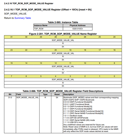
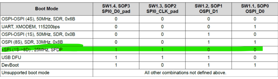
The bootmode is selected as QSPI mode on the SOP pins

image.png

UART Logs when PORz is pressed:

01aefc36abc625f8da980be8cd275a58eb77c6b83fc91c7548a793be4c020c2cded676ddf26b3db6361bf5fc01d7f3e71abc5cfc2b0ce553497c36284fa66dfbd00000000000000000000000000000000000000000000000000000000000000000000000000000000000000000000000000000000000000000000000000000000647d19024398ce5eb0943ddd0f36ec77f3718c0243c773054da7c3cf6d5791fa9a73cc0c8aa4542f0d85d215deaf8059830ab3ce60613fe3585b984dd8933c21CC


It looks a like going to fallback option as UART.


Please do suggest the 

  • Hi ,

    As per the image your have shared the BOOT mode you have set is XSPI bootmode. Here ROM tries to read the SFDP table of flash in 1s bootmode and tries to switch to 8D bootmode upon success. If fails it defaults to 1s boot mode and try to boot in 1S. In you case since flash is QSPI 8D switch will fail. And ROM default to boot in 1S mode.

    We are able to flash and boot from QSPI (S25FL064)when full power cycle is done.
    1. Can you please tell me which SBL + application  are you running. 
    2. In your board have we made sure that flash is reset along with PORz and WarmReset? 
    3. Does S25FL064 package used have a dedicated reset line ?
    4. Is the secondary bootloader or application setting flash into 4 byte addressmode?
      1. If yes please set the flash to only 3 byte addressing mode (Flash is 64Mb = addressable with 3 bytes of address)
      2. The above 3 byte requirements comes from the below requirement in ROM

    Thanks & Regards,
    Rijohn

  • Hi Rijohn,

    1. SBL:  I have rebuilt the sbl_ospi_multicore_elf_am261x-lp_r5fss0-0_nortos_ti-arm-clang source with uploading the JSON file for Flash 

     The Flash JSON file prepared/extracted using the ospi_flash_diag_am261x-lp_r5fss0-0_nortos_ti-arm-clang example.

    2. Yes, Flash will reset when PORZ reset assert

    3. Yes, Reset line is connected to OSPI0_RESET_OUT0/OSPI Reset Pin in syscfg file

    4.Yes, 4 byte is enabled 


      Json

    {

    "flashSize": 8388608,

    "flashPageSize": 256,

    "flashManfId": "0x01",

    "flashDeviceId": "0x6017",

    "flashBlockSize": 65536,

    "flashSectorSize": 4096,

    "cmdBlockErase3B": "0xD8",

    "cmdBlockErase4B": "0xDC",

    "cmdSectorErase3B": "0x20",

    "cmdSectorErase4B": "0x21",

    "protos": {

    "p111": {

    "isDtr": false,

    "cmdRd": "0x03",

    "cmdWr": "0x02",

    "modeClksCmd": 0,

    "modeClksRd": 0,

    "dummyClksCmd": 0,

    "dummyClksRd": 0,

    "enableType": "0",

    "enableSeq": "0x00",

    "dummyCfg": null,

    "protoCfg": null,

    "strDtrCfg": null

    },

    "p112": {

    "isDtr": false,

    "cmdRd": "0x3B",

    "cmdWr": "0x02",

    "modeClksCmd": 0,

    "modeClksRd": 0,

    "dummyClksCmd": 0,

    "dummyClksRd": 8,

    "enableType": "0",

    "enableSeq": "0x00",

    "dummyCfg": null,

    "protoCfg": null,

    "strDtrCfg": null

    },

    "p114": {

    "isDtr": false,

    "cmdRd": "0x6C",

    "cmdWr": "0x34",

    "modeClksCmd": 0,

    "modeClksRd": 0,

    "dummyClksCmd": 0,

    "dummyClksRd": 8,

    "enableType": "5",

    "enableSeq": "0x00",

    "dummyCfg": null,

    "protoCfg": null,

    "strDtrCfg": null

    },

    "p118": {

    "isDtr": false,

    "cmdRd": "0x7C",

    "cmdWr": "0x84",

    "modeClksCmd": 0,

    "modeClksRd": 0,

    "dummyClksCmd": 0,

    "dummyClksRd": 0,

    "enableType": "255",

    "enableSeq": "0x00",

    "dummyCfg": null,

    "protoCfg": null,

    "strDtrCfg": null

    },

    "p444s": {

    "isDtr": false,

    "cmdRd": "0xEB",

    "cmdWr": "0x02",

    "modeClksCmd": 0,

    "modeClksRd": 2,

    "dummyClksCmd": 0,

    "dummyClksRd": 8,

    "enableType": "5",

    "enableSeq": "0x02",

    "dummyCfg": {

    "isAddrReg": false,

    "cmdRegRd":"0x00",

    "cmdRegWr":"0x00",

    "cfgReg":"0x00000000",

    "shift":0,

    "mask":"0x00",

    "bitP":0

    },

    "protoCfg": {

    "isAddrReg": false,

    "cmdRegRd": "0x00",

    "cmdRegWr": "0x00",

    "cfgReg": "0x00000000",

    "shift": 0,

    "mask": "0x00",

    "bitP": 0

    },

    "strDtrCfg": {

    "isAddrReg": false,

    "cmdRegRd": "0x00",

    "cmdRegWr": "0x00",

    "cfgReg": "0x00000000",

    "shift": 0,

    "mask": "0x00",

    "bitP": 0

    }

    },

    "p444d": {

    "isDtr": false,

    "cmdRd": "0xEB",

    "cmdWr": "0x02",

    "modeClksCmd": 0,

    "modeClksRd": 2,

    "dummyClksCmd": 0,

    "dummyClksRd": 8,

    "enableType": "5",

    "enableSeq": "0x02",

    "dummyCfg": {

    "isAddrReg": false,

    "cmdRegRd":"0x00",

    "cmdRegWr":"0x00",

    "cfgReg":"0x00000000",

    "shift":0,

    "mask":"0x00",

    "bitP":0

    },

    "protoCfg": {

    "isAddrReg": false,

    "cmdRegRd": "0x00",

    "cmdRegWr": "0x00",

    "cfgReg": "0x00000000",

    "shift": 0,

    "mask": "0x00",

    "bitP": 0

    },

    "strDtrCfg": {

    "isAddrReg": false,

    "cmdRegRd": "0x00",

    "cmdRegWr": "0x00",

    "cfgReg": "0x00000000",

    "shift": 0,

    "mask": "0x00",

    "bitP": 0

    }

    },

    "p888s": null,

    "p888d": null,

    "pCustom": {

    "fxn": null

    }

    },

    "addrByteSupport": "1",

    "fourByteAddrEnSeq": "0xA1",

    "cmdExtType": "NONE",

    "resetType": "0x10",

    "deviceBusyType": "1",

    "cmdWren": "0x06",

    "cmdRdsr": "0x05",

    "srWip": 0,

    "srWel": 1,

    "cmdChipErase": "0xC7",

    "rdIdSettings": {

    "cmd": "0x9F",

    "numBytes": 5,

    "dummy4": 0,

    "dummy8": 0

    },

    "xspiWipRdCmd": "0x00",

    "xspiWipReg": "0x00000000",

    "xspiWipBit": 0,

    "flashDeviceBusyTimeout": 56000000,

    "flashPageProgTimeout": 448

    }

  • Hi Rijohn,

    I have removed the 4 byte addressing and rebuilt the SBL and tested.

    Still the QSPI boot is not as expected.

    The Resolved is clicked by mistake , due to low internet connectivity 

    Please do check and update the any option i have to try.

  • Hi Rijohn,

    I have removed the 4 byte addressing and rebuilt the SBL and tested.

    Still the QSPI boot is not as expected.

    The Resolved is clicked by mistake , due to low internet connectivity 

    Please do check and update the any option i have to try.

  • Hi Mallikarjuanreddy,

    Since you are using a QSPI flash. Please change the boot mode to 0000 - 4S QSPI boot mode.

    Also, Can you please share the schematic between MCU and QSPI flash and Flash reset architecture?

    Thanks & Regards,
    Rijohn

  • Hi

    Since you are using a QSPI flash. Please change the boot mode to 0000 - 4S QSPI boot mode.

    1. I have changed the boot mode to 0000 , now nothing is booting.

    is there any setting to be changed in the  sbl_ospi_multicore_elf_am261x-lp_r5fss0-0_nortos_ti-arm-clang like in syscfg file to suit the Flash. Also i have shared the JSON file for reference ( earlier.)

  • Hi Mallikarjuanreddy,

    Thank you for the quick response.

    SFDP read happens in 1s mode. Hence we can that communication with Flash works in Devboot mode and 1s mode works.
    Can you reconfirm this by setting bootmode to1S?

    Can you please share the schematic showing connections between MCU and QSPI flash, Flash reset architecture and BOOTMODE SOP pin settings?

    The below are various command issues by ROM in various boot modes

    BOOTMODE  COMMAND ISSUED BY ROM
    OSPI (8S) 0x8B
    QUAD READ (4S) 0x6B
    OSPI (1S) 0x0B
    OSPI (8D)  Starts Boot in 1s -> then Reads SFDP and switches to 8D

    Please refer to Section 5.4.1 in AM261x TRM to for details regarding COMMAND send from ROM during boot in various boot modes.


    As per the json file shared flash uses 0xEB for read. But ROM issues 0x6B command during 4S bootmode.
    Can you please check if the flash supports the command 0x6B ?

    Thanks & Regards,
    Rijohn

  • PORz Signal flow.pdf

    Please find the snip of the schematic to see the Reset flow and pin mux connection

  • Hi 

    I have checked the Datasheet the QSPI supports the 0x6B command.

    Also i have modified the JSON file to suit the QSPI commands to suit 1-1-4

                "p114": {

                        "isDtr": false,

                        "cmdRd": "0x6B",

                        "cmdWr": "0x34",

                        "modeClksCmd": 0,

                        "modeClksRd": 0,

                        "dummyClksCmd": 0,

                        "dummyClksRd": 8,

                        "enableType": "255",

                        "enableSeq": "0x00",

                        "dummyCfg": null,

                        "protoCfg": null,

                        "strDtrCfg": null

                },
    With this option, still the MCU is not booting in any mode
    and in 1S mode log shows as
    Failed to enable OSPI Reset Signal
    Failed to enable the ospi reset line!

    Starting OSPI Bootloader ...
    Some tests have failed!!
    in other mode:
    000000000000000000000000000000000000000000000000000000000000000000000000000000000000000000000647d19024398ce5eb0943ddd0f36ec77f3718c0243c773054da7c3cf6d5791fa9a73cc0c8aa4542f0d85d215deaf8059830ab3ce60613fe3585b984dd8933c21CCC
  • Hi Mallikarjuanreddy,

    Thank you for sharing the schematic snippets!

    1. Can  you please tell me which PIN/Ball from MCU side is connected to QSPI0_RESET_OUTn?
    2. Which version of SDK are you using?
    3. Can you please share section of SOP bootmode switches in schematic? (pull ups and pull downs)
    4. Also can you please confirm if the below in board:
      1. R211 - DNI
      2. R215 - DNI
      3. QSPI_D2 pulled up to VOUT3v3 via R216 10k Pull up.
      4. QSPI_D3 pulled up to VOUT3v3 via R217 10k Pull up.
      5. R220 is populated.
      6. R361 is populated.

    5. Confirm the BOOTMODE from connecting to R5F0 and check the value of register - TOP_RCM_SOP_MODE_VALUE 
    6. Can you please share a scope shot which contains: -> This to confirm if the power up sequencing is correct 
      1. SCOPE SHOT1
        1. 3V3 RAMP
        2. 1V2 RAMP
        3. PORz release.
        4. MCU_WARMRSTn release.

      2. SCOPE SHOT2
        1. PORz Release
        2. MCU_WARMRSTn release.
        3. QSPI_RESETn near QSPI flash side.

      3. SCOPE SHOT3 - [optional] 
        1. SOP[3:0]
        2. PORz

    All the above steps are to reconfirm if the Hardware side is clean. I am suspecting OSPI Reset is not propagated correctly to flash.

    From Software side lets first confirm the flash functionality and json correctness in DEVBOOT mode using ospi_flash_io example.
    Then we will use the same json in SBL and application.


    Thanks & Regards,
    Rijohn

  • Hi Mallikarjuanreddy,

    Before the above steps, can you set the device to UART boot mode and send me the FULL UART terminal log?

    Thanks & Regards,
    Rijohn

  • Hi 

    Please find the UART Logs

    000002010100000000000100414d323631580000000000000400cdab0000010001000000000000000000000000000000000000001aefc36abc625f8da980be8cd275a58eb77c6b83fc91c7548a793be4c020c2cded676ddf26b3db6361bf5fc01d7f3e71abc5cfc2b0ce553497c36284fa66dfbd00000000000000000000000000000000000000000000000000000000000000000000000000000000000000000000000000000000000000000000000000000000647d19024398ce5eb0943ddd0f36ec77f3718c0243c773054da7c3cf6d5791fa9a73cc0c8aa4542f0d85d215deaf8059830ab3ce60613fe3585b984dd8933c21CCCCCCC

  • Hi Mallikarjuanreddy,

    Thank you!

    SOCID_PARSER log looks fine. 


    Thanks & Regards,
    Rijohn

  • Hi 

    in the ospi_flash_io example 

    with 1S mode

    Cortex_R5_0: Failed to enable OSPI Reset Signal

    Cortex_R5_0: Failed to enable the ospi reset line!

    Cortex_R5_0: All tests have passed!!

    with 4S mode 

    Cortex_R5_0: Failed to enable OSPI Reset Signal

    Cortex_R5_0: Failed to enable the ospi reset line!

    Cortex_R5_0: ERROR: ospi_flash_io_compare_buffers:174: OSPI read data mismatch !!!

    Cortex_R5_0: ERROR: ospi_flash_io_compare_buffers:174: OSPI read data mismatch !!!

    Cortex_R5_0: Some tests have failed!!

  • HI 

    GPIO20/D8 - QSPI0_RESET_OUTn

  • Hi Mallikarjuanreddy,

    Thank you for sharing the logs.

    and in 1S mode log shows as
    Failed to enable OSPI Reset Signal
    Failed to enable the ospi reset line!

    RBL does not have an issue. Boot has reached SBL stage.

    Log states that SBL failed because it was not able to issue reset to flash. This could be because of the difference in the reset architecture to the flash in the Launchpad (depending on the version of SDK used). Latest SDK + LP has direct reset to flash using OSPI0_RESET_OUT signal from controller ANDed with WARMRESETn pin. 


    The package we are using is ZEJ package where OSPI0_RESET_OUT0 comes through GPIO20/D8 pin. 
    In AM261x LP - package present is ZFG package . Here the OSPI0_RESET_OUT0 is brought out through GPIO61/K4 in LP-AM261x schematics.


    Ensure to migrate the sysconfig to ZEJ package and configure the QSPI pins as per the connections in your custom board.


    In our case, The QSPI flash does not have a dedicated reset line rather it is multiplexed with IO3 line. And since the size of flash is only 8MB - which is addressable by 3 byte address mode itself , it is technically fine to not issue a dedicated reset to flash. (provided we are not switching to 4 byte address mode). 

    We can remove this OSPI_Reset to flash in hardware but before that just disable this pin in SysConfig and remove all Software calls for flash reset in code base.

    Removal of R220 is recommended so that High State of this pin (due to pull up R204) does not affect the OSPI IO3 data transactions in 4s mode in highspeed mode of flash operations. For now just disable in SW and test.

    Lets proceed the debug from SW side in the below manner.

    1. Testing 1s BOOTMODE
      1. SET protocol in SBL as 1s-1s-1s
      2. Disable 4 byte mode
      3. In the OSPI section in SysConfig ensure to disable OSPI Pins D4- D7, Data Strobe Pin, ECC Fail Pin and OSPI Reset Pin.
      4. Enable DAC
      5. Comment out the board_flash_reset API in the ospi_flash_io.c file
      6. Rebuild the project
      7. Run.

    2. TESTING boot in 4s Bootmode
      1. SET protocol in SBL as 1s-1s-4s
      2. Disable 4 byte mode
      3. In the OSPI section in Sysconfig ensure to disable OSPI Pins D4- D7, Data Strobe Pin, ECC Fail Pin and OSPI Reset Pin.
      4. Enable DAC
      5. Load flash json with correct read and write commands and dummy cycles.
      6. Ensure QE enable type is 5.
        1. As per TRM section 5.4.1.3.1 OSPI (4S) Bootloader Operation  for 1s-1s-4s mode to work 
      7. Comment out the board_flash_reset API in the ospi_flash_io.c, same as in 1s-1s-1s mode
      8. Rebuild the Project
      9. Run

        NOTE: If data integrity issue occur in 4s mode after following above steps try removing R220 resistor and recheck.

    Thanks & Regards,
    Rijohn