


Part Number: AM62P
Hi,
I am trying to run DDR tests on the SK-AM62P-LP EVM board.
I have successfully done the steps described in this post: AM62P: AM62P DDR tests: Error -1170 @ 0x0 Unable to access the DAP. - Arm-based microcontrollers forum - Arm-based microcontrollers - TI E2E support forums
I am able to connect to the board with the XDS110 Debug probe using JTAG, and I can see the DDR test scripts.
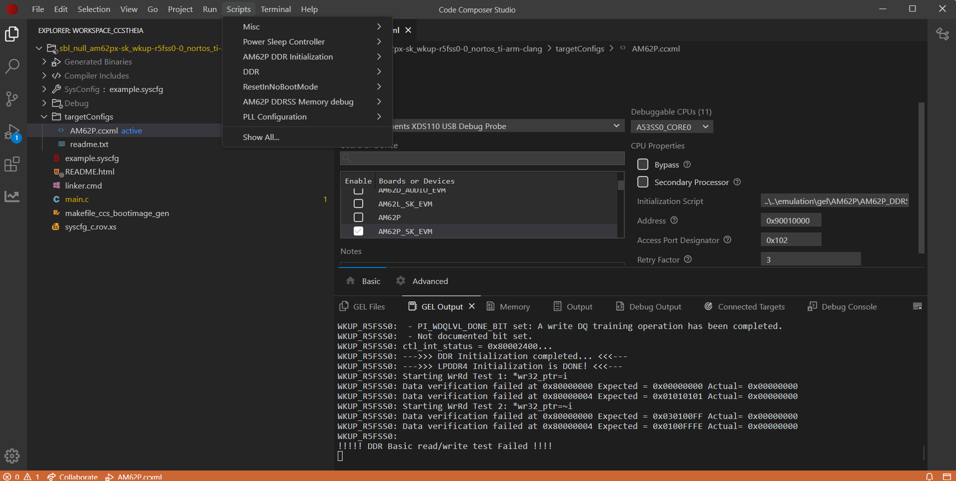
I can successfully run Scripts -> AM62 DDR Initialization -> AM62P_DDR_Initialization_ECC_Disabled.
However, when I try to run Scripts > AM62P DDRSS Memory Debug > Data Tests > Data_WrRd_test, I get:
!!!!! DDR Basic read/write test Failed !!!!
I am using a fresh install of CCS 20.5.1, I have not modified any DDR timing/config parameters, and I am using the out-of-box files provided with CCS.
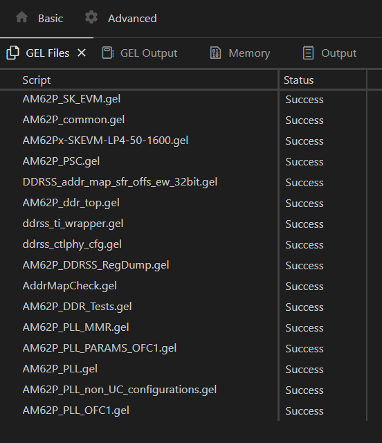
Here is the full GEL Output:
WKUP_R5FSS0: ***WARNING: Please close all Memory Browser Windows before attempting to initialize DDR with GELsWKUP_R5FSS0: Running from R5WKUP_R5FSS0:
DDR not initialized with R5 connect.
Go to menu Scripts --> AM62 DDR Initialization -> AM62P_DDR_Initialization_ECC_Disabled to initialize DDR.
====
WKUP_R5FSS0: --->>> ECC Disabled! <<<---WKUP_R5FSS0: --->>> LPDDR4 Initialization is in progress ... <<<---WKUP_R5FSS0: --->>> DDR controller programming in progress.. <<<---WKUP_R5FSS0: --->>> DDR controller programming completed... <<<---WKUP_R5FSS0: --->>> DDR PI programming in progress.. <<<---WKUP_R5FSS0: --->>> DDR PI programming completed... <<<---WKUP_R5FSS0: --->>> Set PHY registers for all FSPs simultaneously (multicast)... <<<---WKUP_R5FSS0: --->>> DDR PHY Data Slice 0 programming in progress.. <<<---WKUP_R5FSS0: --->>> DDR PHY Data Slice 0 programming completed... <<<---WKUP_R5FSS0: --->>> DDR PHY Data Slice 1 programming in progress.. <<<---WKUP_R5FSS0: --->>> DDR PHY Data Slice 1 programming completed... <<<---WKUP_R5FSS0: --->>> DDR PHY Data Slice 2 programming in progress.. <<<---WKUP_R5FSS0: --->>> DDR PHY Data Slice 2 programming completed... <<<---WKUP_R5FSS0: --->>> DDR PHY Data Slice 3 programming in progress.. <<<---WKUP_R5FSS0: --->>> DDR PHY Data Slice 3 programming completed... <<<---WKUP_R5FSS0: --->>> DDR PHY Address Slice 0 programming in progress.. <<<---WKUP_R5FSS0: --->>> DDR PHY Address Slice 0 programming completed... <<<---WKUP_R5FSS0: --->>> DDR PHY Address Slice 1 programming in progress.. <<<---WKUP_R5FSS0: --->>> DDR PHY Address Slice 1 programming completed... <<<---WKUP_R5FSS0: --->>> DDR PHY Address slice 2 programming in progress.. <<<---WKUP_R5FSS0: --->>> DDR PHY Address Slice 2 programming completed... <<<---WKUP_R5FSS0: --->>> DDR PHY programming in progress.. <<<---WKUP_R5FSS0: --->>> DDR PHY programming completed... <<<---WKUP_R5FSS0: Running from R5 or A53WKUP_R5FSS0: Setting MAIN_PLL12_HSDIV0_CLKOUT_25MHzWKUP_R5FSS0: Setting PLL in integer modeWKUP_R5FSS0: Waiting for Calibration Lock...WKUP_R5FSS0: Cal lockedWKUP_R5FSS0: Waiting for PLL Lock...WKUP_R5FSS0: PLL is locked.WKUP_R5FSS0: MAIN_PLL12_HSDIV0_CLKOUT set.WKUP_R5FSS0: --->>> Set DDR to 25MHz for FSP F0... <<<---WKUP_R5FSS0: --->>> DDR PI initialization started... <<<---WKUP_R5FSS0: --->>> DDR CTL initialization started... <<<---WKUP_R5FSS0: --->>> Inside DDR_Change_freq_ack function ... <<<---WKUP_R5FSS0: --->>> Waiting for first frequency change request ... <<<---WKUP_R5FSS0: Waiting for clock change request... WKUP_R5FSS0: Iter 1: Frequency change request type 2 received from controller WKUP_R5FSS0: Running from R5 or A53WKUP_R5FSS0: Setting MAIN_PLL12_HSDIV0_CLKOUT_800MHzWKUP_R5FSS0: Setting PLL in integer modeWKUP_R5FSS0: Waiting for Calibration Lock...WKUP_R5FSS0: Cal lockedWKUP_R5FSS0: Waiting for PLL Lock...WKUP_R5FSS0: PLL is locked.WKUP_R5FSS0: MAIN_PLL12_HSDIV0_CLKOUT set.WKUP_R5FSS0: Setting the FSP ack bit...WKUP_R5FSS0: Waiting for the request to go away...WKUP_R5FSS0: Clearing the ack bit...WKUP_R5FSS0: Waiting for clock change request... WKUP_R5FSS0: Iter 2: Frequency change request type 0 received from controller WKUP_R5FSS0: Running from R5 or A53WKUP_R5FSS0: Setting MAIN_PLL12_HSDIV0_CLKOUT_25MHzWKUP_R5FSS0: Setting PLL in integer modeWKUP_R5FSS0: Waiting for Calibration Lock...WKUP_R5FSS0: Cal lockedWKUP_R5FSS0: Waiting for PLL Lock...WKUP_R5FSS0: PLL is locked.WKUP_R5FSS0: MAIN_PLL12_HSDIV0_CLKOUT set.WKUP_R5FSS0: Setting the FSP ack bit...WKUP_R5FSS0: Waiting for the request to go away...WKUP_R5FSS0: Clearing the ack bit...WKUP_R5FSS0: Waiting for clock change request... WKUP_R5FSS0: Iter 3: Frequency change request type 2 received from controller WKUP_R5FSS0: Running from R5 or A53WKUP_R5FSS0: Setting MAIN_PLL12_HSDIV0_CLKOUT_800MHzWKUP_R5FSS0: Setting PLL in integer modeWKUP_R5FSS0: Waiting for Calibration Lock...WKUP_R5FSS0: Cal lockedWKUP_R5FSS0: Waiting for PLL Lock...WKUP_R5FSS0: PLL is locked.WKUP_R5FSS0: MAIN_PLL12_HSDIV0_CLKOUT set.WKUP_R5FSS0: Setting the FSP ack bit...WKUP_R5FSS0: Waiting for the request to go away...WKUP_R5FSS0: Clearing the ack bit...WKUP_R5FSS0: Waiting for clock change request... WKUP_R5FSS0: Iter 4: Frequency change request type 0 received from controller WKUP_R5FSS0: Running from R5 or A53WKUP_R5FSS0: Setting MAIN_PLL12_HSDIV0_CLKOUT_25MHzWKUP_R5FSS0: Setting PLL in integer modeWKUP_R5FSS0: Waiting for Calibration Lock...WKUP_R5FSS0: Cal lockedWKUP_R5FSS0: Waiting for PLL Lock...WKUP_R5FSS0: PLL is locked.WKUP_R5FSS0: MAIN_PLL12_HSDIV0_CLKOUT set.WKUP_R5FSS0: Setting the FSP ack bit...WKUP_R5FSS0: Waiting for the request to go away...WKUP_R5FSS0: Clearing the ack bit...WKUP_R5FSS0: Waiting for clock change request... WKUP_R5FSS0: Iter 5: Frequency change request type 2 received from controller WKUP_R5FSS0: Running from R5 or A53WKUP_R5FSS0: Setting MAIN_PLL12_HSDIV0_CLKOUT_800MHzWKUP_R5FSS0: Setting PLL in integer modeWKUP_R5FSS0: Waiting for Calibration Lock...WKUP_R5FSS0: Cal lockedWKUP_R5FSS0: Waiting for PLL Lock...WKUP_R5FSS0: PLL is locked.WKUP_R5FSS0: MAIN_PLL12_HSDIV0_CLKOUT set.WKUP_R5FSS0: Setting the FSP ack bit...WKUP_R5FSS0: Waiting for the request to go away...WKUP_R5FSS0: Clearing the ack bit...WKUP_R5FSS0: --->>> Frequency Change request handshake is completed... <<<---WKUP_R5FSS0: pi_int_status = 0x27C02001...WKUP_R5FSS0: - PI_INIT_DONE_BIT set: The power-on initialization training in PI has been completed.WKUP_R5FSS0: - PI_LVL_DONE_BIT set: The leveling operation has completed.WKUP_R5FSS0: - PI_RDLVL_GATE_DONE_BIT set: A read leveling gate training operation has been completed.WKUP_R5FSS0: - PI_RDLVL_DONE_BIT set: A read leveling operation has been completed.WKUP_R5FSS0: - PI_WRLVL_DONE_BIT set: A write leveling operation has been completed.WKUP_R5FSS0: - PI_CALVL_DONE_BIT set: A CA training operation has been completed.WKUP_R5FSS0: - PI_WDQLVL_DONE_BIT set: A write DQ training operation has been completed.WKUP_R5FSS0: - Not documented bit set.WKUP_R5FSS0: ctl_int_status = 0x80002400...WKUP_R5FSS0: --->>> DDR Initialization completed... <<<---WKUP_R5FSS0: --->>> LPDDR4 Initialization is DONE! <<<---WKUP_R5FSS0: Starting WrRd Test 1: *wr32_ptr=i WKUP_R5FSS0: Data verification failed at 0x80000000 Expected = 0x00000000 Actual= 0x00000000WKUP_R5FSS0: Data verification failed at 0x80000004 Expected = 0x01010101 Actual= 0x00000000WKUP_R5FSS0: Starting WrRd Test 2: *wr32_ptr=~i WKUP_R5FSS0: Data verification failed at 0x80000000 Expected = 0x030100FF Actual= 0x40007300WKUP_R5FSS0: Data verification failed at 0x80000004 Expected = 0x0100FFFE Actual= 0x41004100WKUP_R5FSS0: !!!!! DDR Basic read/write test Failed !!!!
Given that DDR initialization completes successfully and all training steps report done, I was expecting the basic read/write test to pass without needing any modifications.
Has anyone seen this behavior on the SK-AM62P-LP EVM with the default GEL configuration?
Could I be missing a required step?
