AM2434: GPMC timing parameters setting issue

Part Number: AM2434
Other Parts Discussed in Thread: SYSCONFIG, AM6442, AM62P

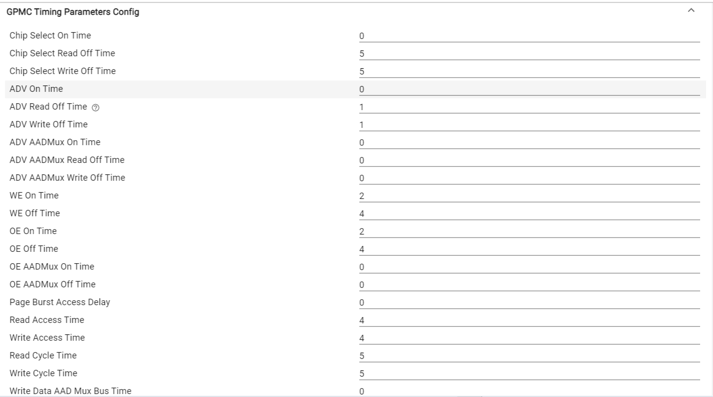
we have interfaced NAND Flash MT29F8G08ABACAWP-IT-C  with AM2434BSFFHIALVR controller  on our custom board.In the Sysconfig we need to fill the timing parameters whose values are not directly available in the NAND flash datasheet.The following are the parameter values we have written in Sysconfig as seen in the screenshots attached.Can you verify the timing paramters values which we have written are correct or not?Can you also provide any formulas for each of the parameters according to the NAND flash timings. image.png

image.pngimage.png


  • Hello Kashish Thakur,

    Thank you for your query !

    Refer the below screenshotted example in the AM64x/AM243x GPMC E2E thread:

    (+) AM6442: GPMC access to FPGA, write success, read fail - Processors forum - Processors - TI E2E support forums

    Although related to an A/D multiplexed synchronous NOR Flash interfaced FPGA (and yours is for an asynchronous non-multiplexed attached NAND), the example refers to the common rules for defining timing parameters of the different GPMC hw interface signals.

    For more information on how NAND protocol timings are defined you can refer to the different subsections of the AM64x/AM243x Datasheet / GPMC and NAND Flash — Asynchronous Mode and AM64x / AM243x TRM / Section, NAND Memory Device in Byte or 16-bit Word Stream Mode

    I will try to follow up tomorrow (COB) with further comments on your configuration and parameters.

    Best Regards,

    Anastas Yordanov 

  • Hello Kashish Thakur,

    Sorry for the big time gap in my response.

    I haven't got a feedback from you so far. I just wanted to check if you already had the chance to experiment with some of the AM6442 GPMC timing parameter values in the Sysconfig and on board with the postconfig-  generated code. 

    I would like to apologize if the example E2E thread with GPMC Synchronous communication timings: [FAQ] Tips for configuring Sitara GPMC registers - Processors forum - Processors - TI E2E support forums might have lead to confusion for some of the parameters. I am clarifying now with our GPMC hardware expert which of the calculations remain the same and which are invalid for an asynchronous non-multiplexed NAND configuration.   

    Please let me know if the topic is still actual for you and we shall continue the discussion or we shall rather close this thread ?

    Thank you !

    Best Regards,

    Anastas Yordanov

  • we calculated the timing parameters according to the formulas which you have given but there is no improvement in the NAND Flash

  • Hi Kashish,

    Sorry if the recommended calculations myside did not have the desired impact.

    Is it possible to provide your calculated values ?

    I will follow-up with more information or additional questions tomorrow.

    Thanks

    Best Regards,

    Anastas Yordanov 

  • Hi Kashish,

    as promised I am getting back to you with further points.

    There are some essential points regarding importance of the  GPMC_CONFIG1_1 - GPMC_CONFIG4_7  setup values for the GPMC NAND interface mode of operation of your MT29F8G08ABACAWP-IT-C. 

    Please refer the following sections of the AM64x/AM243x TRM / Section, GPMC NAND Access Description subsections:

    The Section, Chip-Select Configuration for NAND Interfacing in Byte or Word Stream Mode of the AM64x/AM243x TRM states that the MT29F8G08ABACAWP-IT-C timing parameters / modes shall be considered when initializing the: GPMC_CONFIG1_1 through GPMC_CONFIG4_1 bitfield control values, as follows:

    You GPMC_CONFIG1_1 (CS1) parameters should be OK for a NAND Flash memory interface in Byte mode.

    There are some particular rules that sofwtare shall take into account when performing accesses to the 8-bit NAND flash, as per the Section, NAND Device Command and Address Phase Control of the TRM:

    The Command cycles related parameters are covered in the Section, Command Latch Cycle of the TRM:

    The connectivity between the involved signals during a command cycle and responsible bitfields can be inferred from the timing diagram:

    The choice shall be aligned with the interfaced MT29F8G08ABACAWP-IT-C device specific timing values.

    For the Address latch cycle, the involved settings vs address phase timings relation is shown in the NAND Address Latch Cycle timing diagram under the TRM subsection, Address Latch Cycle of  the Section, GPMC NAND Access Description

    For the NAND data write or read phase specific timings and involved GPMC_CONFIG1_1 - GPMC_CONFIG1_6 bitfields you may want to refer to the Section, NAND Device Data Read and Write Phase Control in Stream Mode of the TRM.

    Can you shortly describe what are the exact timing issues you currently observe when interfacing the NAND with your (corrected according my previous posted formulaes)  Sysconfig GPMC driver configuration ?

    Looking forward to your calculated values with which you had no success and answer to my above question ?

    Thanks

    Best Regards,

    Anastas Yordanov

  •  the issue is we are not able to receive the ready busy signal.We probed the lines using logic analyzer and no response on the ready busy signal.The 0xFFh was going to the NAND flash and rest of the CS and other signals were as expected.If our calculated values are wrong then please provide exact values.We are not able to know this is a hardware issue or configuration issue as this is a custom board.

  • Hi Kashish,

    I am a bit behind with the calculations as these days I had a bit more tasks on my list than usual.

    I hope I can follow-up with calculations based data by tomorrow.

    Thank you for your patience !

    Best Regards,

    Anastas Yordanov

  • Hi Kashish,

    Based on GPMC0FCLKDIV = 0 -> i.e. DivBy1 mode and GPMC0_FCLK freq.=133 MHz ( ~7.5 ns clock period)

    please try setting the following timing parameter values in the corresponding GPMC0_CONFIG2_1 - GPMC0_CONFIG6_1 register bitfields:

    Considering MT29F8G08ABACAWP-IT-C parameters we have following AM62P GPMC0 config. values

    NAND Write cycle 

    ================================================

    CSONTIME = 0 ( 0 ns )

    CSWROFFTIME = 5 ( 5 cycles * 7.5 ns = 37.5 ns )

    ADVONTIME = 0  ( 0 ns )

    ADVWROFFTIME = 5  ( 37.5 ns )

    WEONTIME = 0 ( 0 ns )

    WEOFFTIME = 3   ( 22.5 ns )

    WRACCESSTIME = 4 ( 30ns )

    WRCYCLETIME = 5 ( 37.5 ns )

    --------------------------------------------------------------------------------------

    NAND Read cycle 

    =================================================

    CSRDOFFTIME = 6 ( 6 cycles * 7.5 ns = 45 ns )

    ADVRDOFFTIME = 6 ( 45 ns )

    OEONTIME = 0

    OEOFFTIME = 4 ( 30 ns )

    RDACCESSTIME = 5 ( 37.5 ns )

    RDCYCLETIME = 6 ( 45 ns )

    BUSTURNAROUNDTIME = 14 ( 105 ns )

    I am looking forward to your feedback !

    Best Regards,

    Anastas Yordanov

  • Hi Kashish,

    Do you follow the recommended sequence for issuing the command from the AM243x processor to the NAND memory ?

    Is the WAIT0 input stuck active LOW infinitely (constantly busy) after the processor issues 0xFF to the memory ? 

    Is the MT29F8G08ABACAWP-IT-C R/B# pin attached to the AM243x gpmc0_wait0 pin and do you have the recommended pull-up resistor with the appropriate value (see memory datasheet) attached at this pin ?

    From your Sysconfig GPMC window screenshot I do NOT see what is the specified WAITMONITORINGTIME value. Is it 0 cycles ?

    Looking at your previous parameters:

    I can see the ReadAccessTime=4 > ReadCycleTime=3, WriteAccessTime=4 > WriteCycleTime=3 which means you try to access the bus after the R/W access cycle has elapsed.

    The ADV On Time = 4 can NOT be higher than the ADV Read Off Time = 3 or ADV Write Off Time =3.

    Also the ChipSelectReadOffTime=2 and ChipSelectWriteOffTime=2 can not be lower than ReadAccessTime=4 and WriteAccessTime=4.

    For the timing values relations, and more intuitive explanation, please refer the NAND timing diagram  Figures 12-192 through 12-195 from the AM62Px TRM above.

    Important notice on NDA restrictions: It looks like Micron's MT29F8G08ABACAWP-IT-C memory datasheet contains proprietary and confidential data that must NOT be disclosed / discussed in the Arm-based microcontrollers public E2E forum. Thereby I am deleting the above attached AC characteristics tables screenshots. If you'd like to discuss on concrete parameters we can continue on some of the internal forums. Let me know.

    Looking forward to your answers !

    Thank you

    Best Regards,

    Anastas

  • Hi Kashish,

    I am checking if you had the chance to test some updates in the GPMC configuration registers.

    Let me know your thoughts

    With Regards,

    Anastas