Other Parts Discussed in Thread: ADS130E08
Hi,
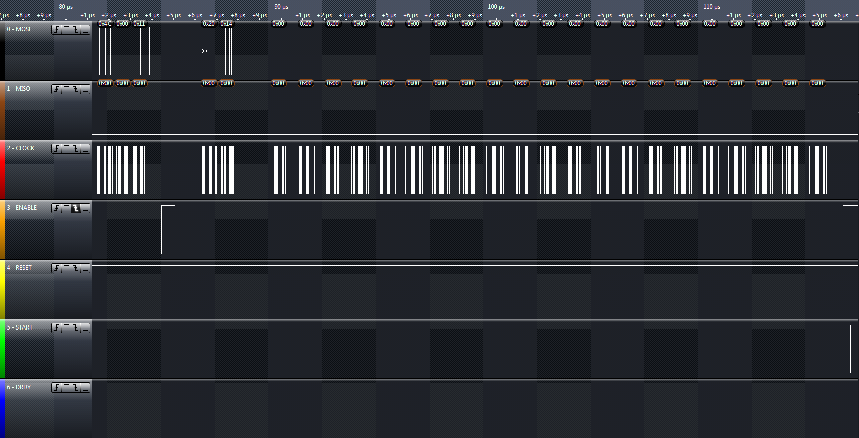
Here is a problem involving two TI products not playing nicely together...
The problem is explained in the last post here.
http://e2e.ti.com/support/data_converters/precision_data_converters/f/73/t/388126
This sounds like a software/firmware issue rather than chip. The chip (from the d/s, Timing Requirements on page 7) should be able to handle up to 20MHz clock for SCLK.
You may want to look at the configuration of the SSI; I would suspect that you may not be reading correctly at the slower speeds even though it may appear that is the case. If at 1.2MHz you don't read all the data, the slower will not read out all the data either.
So far my intuition tells me that there are certain SSI restrictions that are violated. I've followed the recommended protocol as outlined by TI Application Engineers so this problem seems to be a bit more complex. Maybe ssi.c needs to be examined in more detail?
My code:
#include <stdbool.h>
#include <stdint.h>

#include "inc/hw_memmap.h"
#include "inc/hw_ints.h"
#include "inc/hw_gpio.h"
#include "inc/hw_nvic.h"
#include "inc/hw_types.h"

#include "driverlib/gpio.h"
#include "driverlib/interrupt.h"
#include "driverlib/pin_map.h"
#include "driverlib/ssi.h"
#include "driverlib/sysctl.h"
#include "driverlib/systick.h"
#include "driverlib/rom.h"
#include "driverlib/rom_map.h"
#include "driverlib/uart.h"

#include "utils/uartstdio.h"

#include "drivers/pinout.h"
//#include "inc/tm4c1294ncpdt.h"

//*****************************************************************************
//
//!
//! This example uses the following peripherals and I/O signals on EK-TM4C1294XL.
//! You must review these and change as needed for your own board:
//! - SSI0 peripheral
//! - GPIO Port A peripheral (for SSI0 pins)
//! - SSI0CLK - PA2
//! - SSI0Tx  - PA4
//! - SSI0Rx  - PA5
//!
//! - GPIO Port H peripheral (GPIO pin OUT)
//! - CS	  - PH0
//! - RESET	  - PH1
//!
//! - GPIO Port K peripheral (GPIO pin OUT)
//! - START	  - PK6
//!
//! - GPIO Port M peripheral (GPIO pin IN)
//! - DRDY	  - PM6
//!
//! For this example to work, the following connections are needed on the
//! EK-TM4C1294XL evaluation board.
//! - SSI0CLK(PA2) - CLK(3)
//! - SSI0Tx(PA4)  - DIN(11)
//! - SSI0Rx(PA5)  - DOUT(13)
//! - CS(PH0)	   - CS(7)
//! - RESET(PH1)   - RESET(8)
//! - START(PK6)   - START(14)
//! - DRDY(PM6)	   - DRDY(15)
//!
//! The following UART signals are configured only for displaying console
//! messages for this example.  These are not required for operation of SSI0.
//! - UART0 peripheral
//! - GPIO Port A peripheral (for UART0 pins)
//! - UART0RX - PA0
//! - UART0TX - PA1
//!
//
//*****************************************************************************
//
uint32_t g_ui32SysClock;

//Sent Data
uint32_t opcode_tx[1];

uint32_t channel_code[8];

//Received Data
uint32_t cfg_reg[21];
uint32_t rdata_rx[19];
uint32_t rx_stat[3];
uint32_t rx_data[8];
//

//*****************************************************************************
//
// Configure the UART and its pins.  This must be called before UARTprintf().
//
//*****************************************************************************
void ConfigureUART(void) {
	SysCtlPeripheralEnable(SYSCTL_PERIPH_GPIOA);
	SysCtlPeripheralEnable(SYSCTL_PERIPH_UART0);
	GPIOPinConfigure(GPIO_PA0_U0RX);
	GPIOPinConfigure(GPIO_PA1_U0TX);
	GPIOPinTypeUART(GPIO_PORTA_BASE, GPIO_PIN_0 | GPIO_PIN_1);
	UARTStdioConfig(0, 9600, g_ui32SysClock);
}

//*****************************************************************************
//
// This function sets up SPI0 to be used as Master in freescale mode.
//
//*****************************************************************************
void InitSPI0(void) {
	SysCtlPeripheralEnable(SYSCTL_PERIPH_SSI0);
	SysCtlPeripheralEnable(SYSCTL_PERIPH_GPIOA);

	GPIOPinConfigure(GPIO_PA2_SSI0CLK);
	GPIOPinConfigure(GPIO_PA3_SSI0FSS);
	GPIOPinConfigure(GPIO_PA4_SSI0XDAT0);
	GPIOPinConfigure(GPIO_PA5_SSI0XDAT1);

	GPIOPinTypeSSI(GPIO_PORTA_BASE,
			GPIO_PIN_5 | GPIO_PIN_4 | GPIO_PIN_3 | GPIO_PIN_2);

	//ADS SPI settings are CPOL = 0 and CPHA = 1.
	SSIConfigSetExpClk(SSI0_BASE, g_ui32SysClock, SSI_FRF_MOTO_MODE_1,
	SSI_MODE_MASTER, 10000000, 8);

	SSIEnable(SSI0_BASE);
}

//*****************************************************************************
//
// Configure GPIO pins.  This replaces the SSI0Fss with another pin.
//
//*****************************************************************************
void InitGPIO(void) {
	// PH0 - CS
	// PH1 - RESET
	SysCtlPeripheralEnable(SYSCTL_PERIPH_GPIOH);
	GPIOPinTypeGPIOOutput(GPIO_PORTH_BASE, GPIO_PIN_0 | GPIO_PIN_1);
	GPIOPinWrite(GPIO_PORTH_BASE, GPIO_PIN_0, GPIO_PIN_0);
	GPIOPinWrite(GPIO_PORTH_BASE, GPIO_PIN_1, GPIO_PIN_1);

	// PK6 - START
	SysCtlPeripheralEnable(SYSCTL_PERIPH_GPIOK);
	GPIOPinTypeGPIOOutput(GPIO_PORTK_BASE, GPIO_PIN_6);
	GPIOPinWrite(GPIO_PORTK_BASE, GPIO_PIN_6, 0);

	// PM6 - DRDY
	SysCtlPeripheralEnable(SYSCTL_PERIPH_GPIOM);
	GPIOPinTypeGPIOInput(GPIO_PORTM_BASE, GPIO_PIN_6);
}


//*****************************************************************************
//
// Write to SPI
//
//*****************************************************************************
void spi_write(uint32_t len, uint32_t pui32DataTx[]) {

	uint32_t ui32Index;
	uint32_t pui32DataRx[19];

	//
	// Read any residual data from the SSI port.  This makes sure the receive
	// FIFOs are empty, so we don't read any unwanted junk.  This is done here
	// because the SPI SSI mode is full-duplex, which allows you to send and
	// receive at the same time.  The SSIDataGetNonBlocking function returns
	// "true" when data was returned, and "false" when no data was returned.
	// The "non-blocking" function checks if there is any data in the receive
	// FIFO and does not "hang" if there isn't.
	//
	while (SSIDataGetNonBlocking(SSI0_BASE, &pui32DataRx[0])) {
	}

	for (ui32Index = 0; ui32Index < len; ui32Index++) {
		//
		// Send the data using the "blocking" put function.  This function
		// will wait until there is room in the send FIFO before returning.
		// This allows you to assure that all the data you send makes it into
		// the send FIFO.
		//
		SSIDataPut(SSI0_BASE, pui32DataTx[ui32Index]);
	}

	//
	// Wait until SSI0 is done transferring all the data in the transmit FIFO.
	//
	while (SSIBusy(SSI0_BASE)) {
	}

}

//*****************************************************************************
//
// Read from SPI
//
//*****************************************************************************
void spi_read(uint32_t rx_len, uint32_t *rx_Data) {

	uint32_t ui32Index;
	uint32_t pui32DataRx[19];

    //
    // Read any residual data from the SSI port.  This makes sure the receive
    // FIFOs are empty, so we don't read any unwanted junk.  This is done here
    // because the SPI SSI mode is full-duplex, which allows you to send and
    // receive at the same time.  The SSIDataGetNonBlocking function returns
    // "true" when data was returned, and "false" when no data was returned.
    // The "non-blocking" function checks if there is any data in the receive
    // FIFO and does not "hang" if there isn't.
    //
    while(SSIDataGetNonBlocking(SSI0_BASE, &pui32DataRx[0]))
    {
    }

    //
    // Read bytes from RX FIFO.
    //
    for(ui32Index = 0; ui32Index < rx_len; ui32Index++)
    {
    	//
    	// Put dummy bytes out to read bytes in
    	//
    	SSIDataPut(SSI0_BASE, 0x00);
        //
        // Receive the data using the "blocking" Get function. This function
        // will wait until there is data in the receive FIFO before returning.
        //
        SSIDataGet(SSI0_BASE, &rx_Data[ui32Index]);
        //
        // Since we are using 8-bit data, mask off the MSB.
        //
        rx_Data[ui32Index] &= 0x00FF;
    }

    //
    // Wait until SSI0 is done transferring all the data in the transmit FIFO.
    //
    while(SSIBusy(SSI0_BASE))
    {
    }

}


//*****************************************************************************
//
// Reads and parses the cell voltage registers
//
//*****************************************************************************
void rdatac_parse(uint32_t rx_data[19], // Controls which cell voltage register is read back.
					uint32_t rx_output[8], // Array of the parsed cell codes
					uint32_t rx_status[3]
					)
{

  uint32_t parsed_cell;
  uint32_t data_counter = 3; //data counter
  uint32_t current_cell;

  	  //a.i
  	  	  for(current_cell = 0; current_cell<3; current_cell++)
  	  	  {
  	  		  rx_status[current_cell] = rx_data[current_cell];
  	  	  }

        //a.ii
		for(current_cell = 0; current_cell<8; current_cell++)	 	// This loop parses the read back data into cell voltages, it
        {														   		  			// loops once for each of the 3 cell voltage codes in the register

          parsed_cell = rx_data[data_counter+1] + (rx_data[data_counter] << 8);//Each cell code is received as two bytes and is combined to
																					 // create the parsed cell voltage code

          rx_output[current_cell] = parsed_cell;
          data_counter = data_counter + 2;											 //Because cell voltage codes are two bytes the data counter
																					//must increment by two for each parsed cell code
        }

}
//*****************************************************************************
//
// Read ADS Registers
//
//*****************************************************************************
void ads_rreg(void){
	//Read all Registers
	uint32_t rregOP[2];
	rregOP[0] = 0x20;
	rregOP[1] = 0x14;
	GPIOPinWrite(GPIO_PORTH_BASE, GPIO_PIN_0, 0); //CS low
	spi_write(2,rregOP);
	spi_read(21, cfg_reg);
	GPIOPinWrite(GPIO_PORTH_BASE, GPIO_PIN_0, GPIO_PIN_0); //CS high
}


//*****************************************************************************
//
// Initialize
//
//*****************************************************************************
void ads_init(void){
	//Reset Pulse
	GPIOPinWrite(GPIO_PORTH_BASE, GPIO_PIN_1, 0);
	SysCtlDelay(10); //minimum pulse width timing specifications
	GPIOPinWrite(GPIO_PORTH_BASE, GPIO_PIN_1, GPIO_PIN_1);
	SysCtlDelay(400); //18 tclk cycles to complete initialization (9252ns ~ 10us)


	//Send SDATAC Command
	opcode_tx[0] = 0x11;
	GPIOPinWrite(GPIO_PORTH_BASE, GPIO_PIN_0, 0); //CS low
	spi_write(1, opcode_tx);
	GPIOPinWrite(GPIO_PORTH_BASE, GPIO_PIN_0, GPIO_PIN_0); //CS high
}

//*****************************************************************************
//
// Write ADS Config Registers
//
//*****************************************************************************
void ads_config(uint32_t config1, uint32_t config2, uint32_t config3){
	uint32_t refconfig1[3];
	uint32_t refconfig2[3];
	uint32_t refconfig3[3];

	//Config1
	refconfig1[0] = 0x41;
	refconfig1[1] = 0x00;
	refconfig1[2] = config1; //0x01
	GPIOPinWrite(GPIO_PORTH_BASE, GPIO_PIN_0, 0); //CS low
	spi_write(3, refconfig1);
	GPIOPinWrite(GPIO_PORTH_BASE, GPIO_PIN_0, GPIO_PIN_0); //CS high

	//Config2
	refconfig2[0] = 0x42;
	refconfig2[1] = 0x00;
	refconfig2[2] = config2; //0x60
	GPIOPinWrite(GPIO_PORTH_BASE, GPIO_PIN_0, 0); //CS low
	spi_write(3, refconfig2);
	GPIOPinWrite(GPIO_PORTH_BASE, GPIO_PIN_0, GPIO_PIN_0); //CS high

	//Config3
	refconfig3[0] = 0x43;
	refconfig3[1] = 0x00;
	refconfig3[2] = config3; //0xC0
	GPIOPinWrite(GPIO_PORTH_BASE, GPIO_PIN_0, 0); //CS low
	spi_write(3, refconfig3);
	GPIOPinWrite(GPIO_PORTH_BASE, GPIO_PIN_0, GPIO_PIN_0); //CS high
}

//*****************************************************************************
//
// Write ADS Config Channels
//
//*****************************************************************************
void ads_chnset(uint32_t channel_code[8]){
	//Set Channel Settings
	uint32_t CHnSET[3];
	CHnSET[0] = 0x45;
	CHnSET[1] = 0x00;
	CHnSET[2] = 0x10;

	uint32_t channel;
	for (channel = 0; channel <8; channel ++)
	{
		CHnSET[2] = channel_code[channel];
		GPIOPinWrite(GPIO_PORTH_BASE, GPIO_PIN_0, 0); //CS low
		spi_write(3, CHnSET);
		GPIOPinWrite(GPIO_PORTH_BASE, GPIO_PIN_0, GPIO_PIN_0); //CS high
		CHnSET[0]++;
	}
}


//*****************************************************************************
//
// MAIN
//
//*****************************************************************************
int main(void) {
	uint32_t read = 0;
	uint32_t i;

	g_ui32SysClock = SysCtlClockFreqSet((SYSCTL_XTAL_25MHZ |
	SYSCTL_OSC_MAIN | SYSCTL_USE_PLL |
	SYSCTL_CFG_VCO_480), 120000000);

	ConfigureUART();
	InitGPIO();
	InitSPI0();

	//Initialize ADS
	UARTprintf("\n\nInitialized. Starting ADS130E08.\n");
	ads_init();

	//Read Registers
	ads_rreg();
//	UARTprintf("\nRREG:");
//    for(i = 0; i < 21; i++){
//    	UARTprintf(" %x,", cfg_reg[i]);
//    }

    //Configure ADS
	ads_config(0x01,0x73,0xcc);
	//INTERNAL DC TEST		- (0x01,0x73,0xcc)
	//INTERNAL PULSED TEST	- (0x01,0x70,0xcc)
	//EXTERNAL MEASURE		- (0x01,0x60,0xcc)

	//Set Channel Settings
	channel_code[0] = 0x10;
	channel_code[1] = 0x11;
	channel_code[2] = 0x11;
	channel_code[3] = 0x11;
	channel_code[4] = 0x11;
	channel_code[5] = 0x11;
	channel_code[6] = 0x11;
	channel_code[7] = 0x11;
	ads_chnset(channel_code);
	//Gain 1	- 0x10
	//Shorted	- 0x11
	//TEST		- 0x15

	//Read Registers
	ads_rreg();
//	UARTprintf("\nRREG:");
//    for(i = 0; i < 21; i++){
//    	UARTprintf(" %x,", cfg_reg[i]);
//    }

    //START
	GPIOPinWrite(GPIO_PORTK_BASE, GPIO_PIN_6, GPIO_PIN_6);
	SysCtlDelay(400); //Wait


	//
	//Read Data Continuously
	//
	//RDATAC
    opcode_tx[0] = 0x10;
	GPIOPinWrite(GPIO_PORTH_BASE, GPIO_PIN_0, 0); //CS low
	spi_write(1, opcode_tx);
	GPIOPinWrite(GPIO_PORTH_BASE, GPIO_PIN_0, GPIO_PIN_0); //CS high

//	UARTprintf("\n\nRDATA CONTINUOUS");
	GPIOPinWrite(GPIO_PORTH_BASE, GPIO_PIN_0, 0); //CS low

	//
//	uint32_t pui32DataRx2[19];
//    while(SSIDataGetNonBlocking(SSI0_BASE, &pui32DataRx2[0]))
//    {
//    }
//	SSIConfigSetExpClk(SSI0_BASE, g_ui32SysClock, SSI_FRF_MOTO_MODE_1,
//	SSI_MODE_MASTER, 2000000, 8);
    //
	read = 1;

	while(1)
    {
//    		UARTprintf("\n\nWaiting for DRDY high........");
    		while(GPIOPinRead(GPIO_PORTM_BASE, GPIO_PIN_6)){
    		//Wait for DRDY to be high
    			read = 0;
    			for(i=0;i<2;i++)
    				read = 0;
    		}
//    		UARTprintf("Done.");
//    		UARTprintf("\nWaiting...");
    		uint32_t pui32DataRx2[19];
    		while(SSIDataGetNonBlocking(SSI0_BASE, &pui32DataRx2[0]))
    		{
    		}

    		do{
    			if (GPIOPinRead(GPIO_PORTM_BASE, GPIO_PIN_6) == 0){
    				spi_read(19, rdata_rx);
    				read = 1;
    				rdata_rx[0]=0;
//    				UARTprintf("Read.");
    			}
    			else{
//    				UARTprintf(".");
    			}
    		}while(read == 0);

//  		rdatac_parse(rdata_rx, rx_data, rx_stat);

//    		UARTprintf("\nReceived :");
//    		for(i = 0; i < 8; i++){
//    	    	UARTprintf(" %i,", rx_data[i]);
//    	    }
//
//    		UARTprintf("\nSTATUS :");
//    	    for(i = 0; i < 3; i++){
//    	    	UARTprintf(" %x,", rx_stat[i]);
//    	    }

    }

	GPIOPinWrite(GPIO_PORTH_BASE, GPIO_PIN_0, GPIO_PIN_0); //CS high

	//
	// Return no errors
	//
	return (0);
}
Thanks,
Stephen