This thread has been locked.

If you have a related question, please click the "Ask a related question" button in the top right corner. The newly created question will be automatically linked to this question.

Glitches on ADC

Other Parts Discussed in Thread: TM4C129ENCPDT

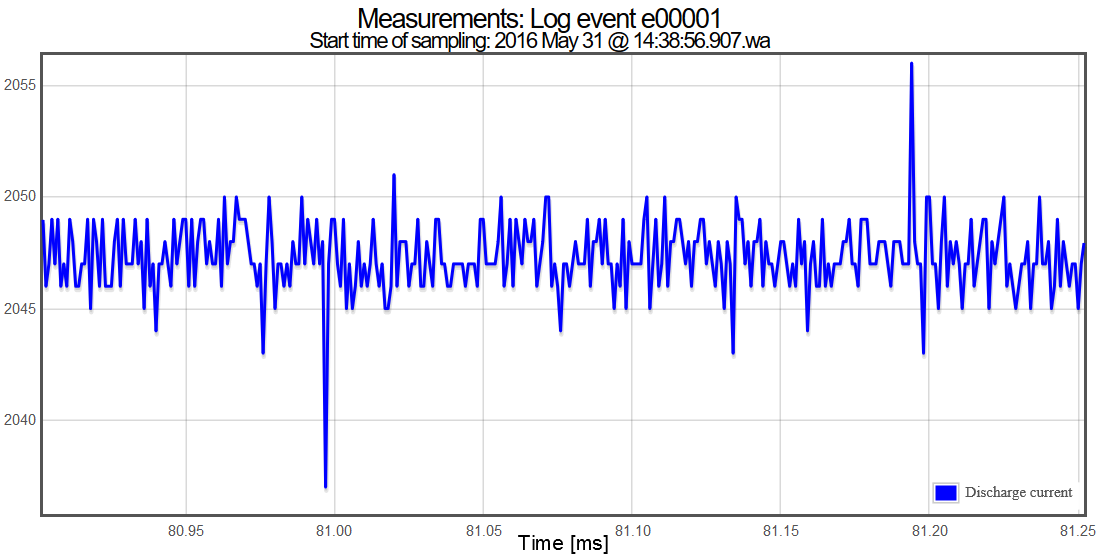
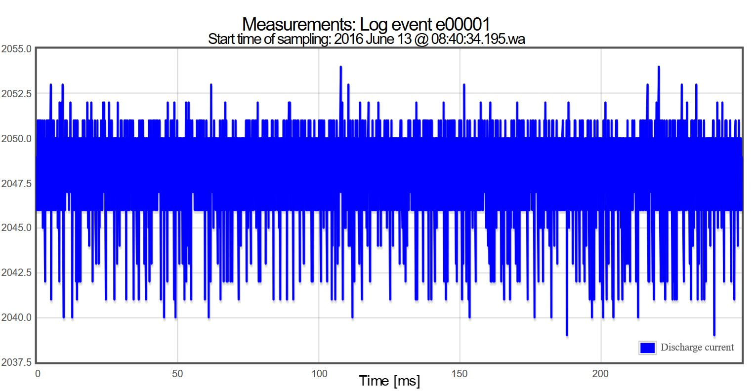
At the Ain2 A/D input, noise spikes are observed at fixed DC input. The device is TM4C129ENCPDT silicon rev 3. See this recording:

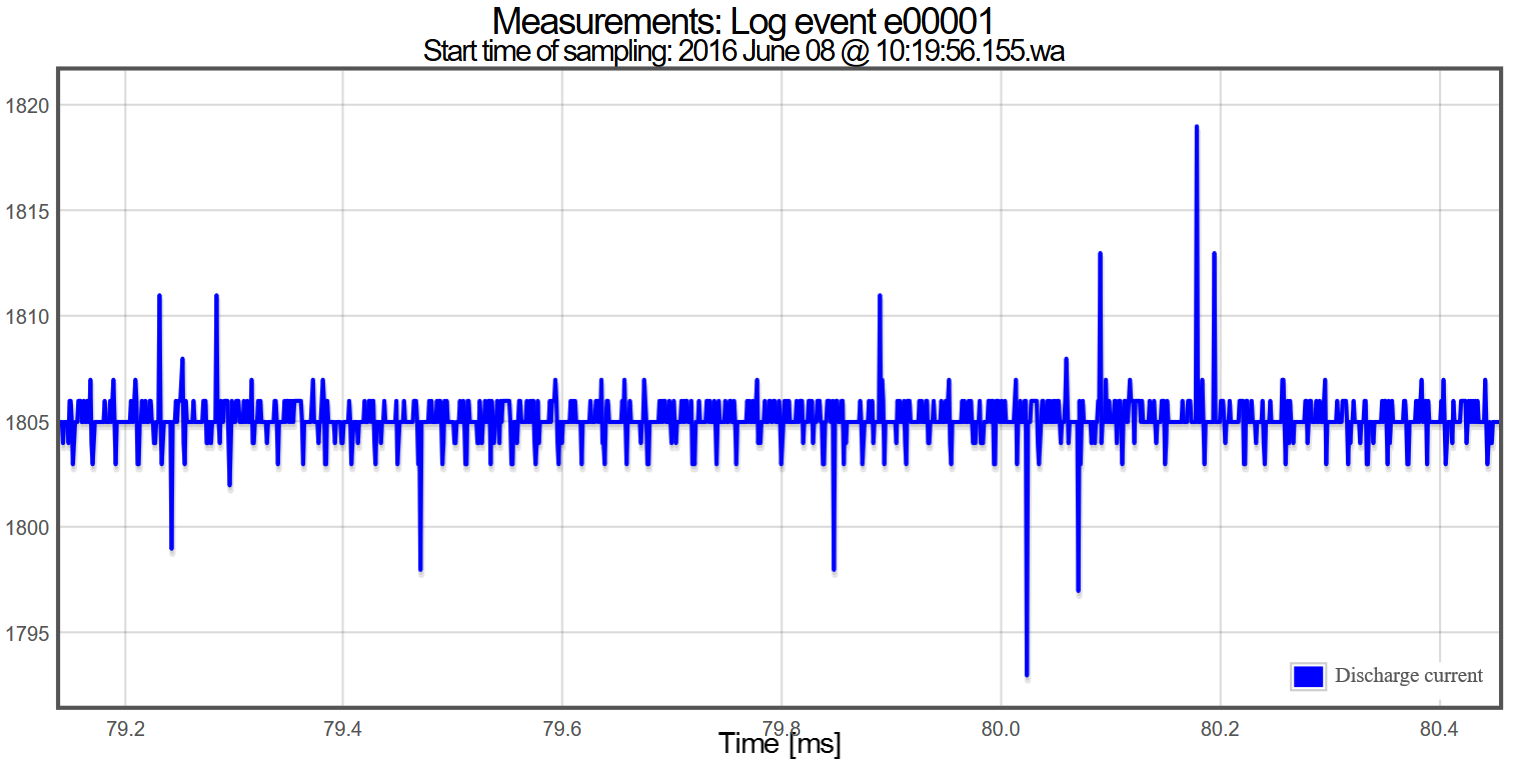
When zooming it looks like this:

The input is a resistive voltage division from the separate power supply (3.3V) for the analog GNDA and VREF+/VDDA. The input is filteret by a 100nF capacitor to GNDA and all components are placed few mm from the device pins. VREFA+ and VDDA pins are tied together. The actual test is for full speed 2 MSPS, but the same result shows for 500 KSPS. I have tried 64 clock Sample/hold but it does not affect these pictures. The errata tells about spikes at the Ain0, but not at the other inputs. The PCB is well designed using 4 layers. The processor is running RTOS and Ethernet traffic at the same time. Configuration is 'ADC_TRIGGER_ALWAYS'.

Any ideas if this is an expected behavior or how to make better performance in terms of noise ?

  • Neat post - I believe 2 (additional) items will "add value:"

    • have you tested for similar upon other boards?   (avoiding single-board anomaly)
    • You note a separate supply for VREF+ and VDDA.  If that's distant from the MCU it must be properly decoupled.  (wise to decouple - anyway)
    • Firm/I always employ small ferrite bead + small & large value filter caps (close) to VDDA.
    • You note a resistive divider - but not your attempt to "match" the input impedance of the MCU's ADC input.

    It would be appreciated if you'd identify that graphing program AND how you imported the MCU's ADC data.   Thank you.

  • Hello Peter,

    To add to cb1's last point, did you try using the Sample and Hold register to increase the time of sampling? Also do note that the ADC has an error which under nominal conditions is set around 2 LSB's

    Regards
    Amit
  •  -good point in testing on more boards- Just did, same story, see picture.

    -Power supply is a few mm from the MCU pins (LP2980-3.3)

    -Small ferrite and large filter caps are in place (1uH, 10uF/100nF)

    -The resistor are simply two 2k6 dividing the 3,3V VDDA supply. 100nF in parallel with lower resistor.

    -good idea to extent sampling time - tried 64 clocks, same result

    We are performing uDMA transfer to some big arrays into a combination of internal RAM and external RAM. An internal transfer generates raw wave files (true data) to output through a web interface as download and direct view as shown here.

  • First 5 counts is not very large, on the order of 0.1% Is your VDDA actually stable to better than that at the frequency you are measuring at? Have you confirmed it? How? This is non-trivial.

    Is GNDA also filtered?

    Check the A/D specs. The 123 is rated at 60dB for SNR at 1kHz or 10bits

    Is your source actually this good? How did you measure to < 0.1%?

    Robert
  • - I have tried to connect the GNDA to the digital gnd through a 600R bead and a 20 ohm resistor, but no major difference.
    - I will now try next week to split VDDA and VREFA+ to try to isolate disturbance into VREFA+
  • Ah, you have a separate reference. What are you using for a reference? How is it buffered?

    The reference actually has fairly significant high frequency demands upon it so the impedance/decoupling needs attention.

    Robert
  • Hi Peter,

    Have noticed similar with EK-TM4C1294-XL launch pad ADC noise is quiet high +vRefA directly tied to +3v3. The odd thing is a good part of the sample noise was coming from +5 feeding +3v3 LDO assume the MCU internal 2v0 LDO.

    The launch pad was powered from computers USB port and +3v3 LDO regular regulator has a 2uf ceramic on the output seemingly was not enough decoupling. The scope revealed 200mv saw tooth wave on +5 feeding the +3v3 LDO. Adding a 47uf electrolytic +5v stopped most all sample noise mostly present in the ADC internal temperature sensor and bleeds into the channel samples. BTW acquisition of stray pulses exiting out the channel from the internal ADC capacitors of SAR type ADC can be coupled to ground via resistor and setting the RC time constant to match expected acquisition times can remove a lot of that noise.

    TI-Analog precision ADC seminar.pdf

  • @BP101, the slides from the old TI seminar was very useful and gave inspiration how to make a better drive circuit for the ADC inputs.

    By having a drive of the ADC input of a voltage divider made by two 2K6 resistors and a 100nF low side capacitor we can clearly see the effect of the internal switching capacitors sending charge back to the external circuit. By changing the voltage division resistor to just 330 ohm the influence from the internal circuit disappeared.

    We have tried to split the VDDA and VREFA+ by having a bead to the VREFA+ and a 100nF capacitor to GNDA. It did not make any change.

    We have tried to switch off the ethernet connection while sampling, but no effect was observed.

    We are using the AIN2 pin (pin 14) so no digital pins nearby.

    We still see these spurious spikes. Obviously anyone can average the result, but we need the actual individual samples at full speed.

    So the question is still open, is this something we will need to accept as normal behavior ?

  • Have you checked you reference and source yet?

    Robert
  • The vcc source is a separate 3,3V supply having beads and capacitors at grund and vcc. The reference test i made was making additional split of VDDA and Vref by bead and capacitor (without effect). I have tried to make measurement by a scope, but it is a difficult task to make sure that what I measure is the real source or noise from the probes. I can see some noise on the scope but difficult to determine if this is from the vcc only. I have tried to use a small extension of paired wire to reach the scope probes in some distance. Any good ideas ?
  • What kind of measurement are you making with the scope? Many are only good to 8 bits so noise of this magnitude wouldn't show up on a DC measurement.

    Your best reference for this would be a battery. That won't be stable long term but should be over short periods to the scale you are working at. There are also relatively inexpensive voltage references available that would give you more choice of voltage levels.

    The reference is also going to be critical, if it's not set up correctly it will also feed noise into the A/D. It needs to be low impedance and capable of high frequencies.

    Also using a 3V3 supply to measure A/D characteristics of an A/D with a 3V3 max is probably a bad idea.

    Robert
  • Hi Peter,

    Sorry to get back later so lately tied in fight with my own demons and have turned a few mile stones - hurray!!

    That divider can also be trade off pulling ground noise so we are using 510 ohm versus your 330 ohm. Calculated a 20pf (.02nf) provided the proper acquisition RC time constant for LM3S SAR ADC but it also caused edge roll off and slows down the step response. It often requires more than 1nf to remove glitches but 100nf sets the record like that's 0.1uf. Perhaps an internal 3/4 filter can remove even more undesired low level noise.   

    You stated to have isolated +VREFA from VDD  via ferrite bead, inferred a high resistance as no mention of adding series resistor for noise rejection. Perhaps try to isolate GNDA with ferrite bead if it is very low resistance 0.02mOhm or less. You noted 10nf filtering +VREFA and .01uf to 1.0uf ceramic capacitor TM4C suggested values (2 parallel capacitors) or 2uf 1uf typical, see note (c) ADC electrical section.   

    ADC samples (not sure if posted yet) ADCCTL REG 38 configuration (+Vref ) internal or external,  default internal reference.

    // Configure both ADC0/1 VREFP external VRefA 3v3 
    ROM_ADCReferenceSet(ADC0_BASE, ADC_REF_EXT_3V);
    ROM_ADCReferenceSet(ADC1_BASE, ADC_REF_EXT_3V);


  • Peter,

    Another thought may not have been yet mentioned and makes a huge difference in the sample quality.

    Setting ADC hardware over sampling 4x will reduce much undesired noise but reduce overall precision but SW filter can be reduced.
    Have rechecked our +VREF/VDDA are coupled to 1.0uf //.01uf + four more 0.1uf caps and 6.8k resistor in series 0.05mOhm ferrite bead go to a 3v3 LDO. Electrical section 2MBPS ADC suggest 440ua max +VREF and 2ua leakage, 6.8k isolation should allow 480ua tops. Oddly it doesn't show VDDA max current and suspect is for the ADC peripheral itself must use less than 440ua.

    I would not suggest driving the MCU or any peripheral directly from a switching supply set 3v3 without an buck down LDO regulator in series. Opinions may vary but my thought, the overshoot often associated with a switcher can be clamped by a series buck 3v3 LDO.

    Differential ADC table 27-45 surprisingly lists VDDA 3.63 max well above VDD but like Robert suggest might not be so good to power separately.
  • Sorry, not battery for a/ d reference but as a voltage input to check.

    Robert
  • Oversampling does not reduce precision.

    Also I was not referring to VDDA max but rather that it is unwise to test with values at that are at the limit of the measuring range. Such measurements are more likely to have artifacts which will overstate or understate the device performance.

    Robert
  • Thank you all for your ideas and inputs.

    Latest test have been:

    - Use of small battery in parallel with 100nF and 2n2F as input to the ADC - no change in signal noise:

    - Adding bead in series with digital supply for the processor - no change

    It seems as if some internal noise is disturbing the conversion. The noise seems without a specific frequency. It might be in the SAR itself as an increase in sample/hold time-clocks does not make any change to the issue.

    It could be of interest if anyone have made a similar setup and having good results ?

    Then at least we could try to replicate such conditions.

  • Peter Johansen said:
    - Use of small battery in parallel with 100nF and 2n2F as input to the ADC - no change in signal noise:

    That was a bit of a long shot but worth the check.

    Peter Johansen said:
    - Adding bead in series with digital supply for the processor - no change

    I wouldn't have expected much from that

    Peter Johansen said:
    It might be in the SAR itself as an increase in sample/hold time-clocks does not make any change to the issue.

    That's why I keep suggesting investigating the reference.

    This is almost certainly a capacitive based SAR. As such it needs to charge and discharge the comparison capacitors multiple times for each conversion (once per bit). So if it takes 1uS for conversion (it's actually faster) you can expect bandwidth requirements on the order of 100MHz for the reference input. And since it is charging and discharging capacitors it is a high current requirement.

    Robert

  • The VDDA is supplied from a separate linear regulator of 3.3V. From this line the VREFA+ is made through a bead and decoupled by 100nF in parallel with 2n2F. All mounted a few mm from the pins. Any better suggestions ?
  • Robert - would not an even larger, paralleled cap (in addition to those listed) assist the delivery of those, "high peak currents" you well noted?

  • That should be good, I'd rather an actual reference unless doing ratiometric conversions but that's an accuracy not a noise issue.

    VDDA should be probably be filtered as well, although I'm not necessarily expecting much improvement from that.

    What you should probably do now is calculate your SNR. I suspect you will find it exceeds the A/D specifications. (IIRC that's 60dB min and 65dB nominal or 9.7 to 10.5 bits)

    Robert
  • Maybe, the problem might be the frequency response of a large cap. Maybe the addition of a 1u, maybe. And the internal caps I would expect to be quite small, smaller than the S/H cap.

    It might be worth attempting to measure the AC on the caps and see if an issue is apparent. Might not be an easy measure to make with any confidence though.

    Robert
  • If the S/N ratio spec. covers what I see, then the processor is doing nearly ok according to spec., but it could be of interest to know if the behavior I see is as expected. If yes, we can finalize this part of our engineering work, if not, we still have a job to do.
  • Always two questions

    1. Is this within spec? You can't depend on exceeding the spec.
    2. How well can I do?  But the spec is usually conservative so you may do better. So, how much time do you want to spend improving a result you cannot guarantee?

    Only TI could answer the spectrum issue with any definiteness. And I think the real question is, Am I missing something I should be doing? I don't think I've any other suggestions but I'll ponder a bit, maybe someone else does.

    Robert

  • >From this line the VREFA+ is made through a bead and decoupled by 100nF in parallel with 2n2F. The resistance of the bead if lower then 3.3k does not provide much of any power supply ripple rejection or isolation.

    Peter the minimum capacitance even with linear supply remains 1.0uf // .01uf, 100nf might not be providing enough backwash filter for +VREFA. However see your point of still not seeing much change even with liner supply. Hardware averaging is said to reduce through put but also from what I have noticed seems to reduces the time following noise and producing SAR samples in lower or higher bit ranges, not sure which ones. The result is a much cleaner sample range with reduced precision. In your case that might be a good thing (less is more) turn down the volume.

    Had a similar issue like your reporting ADC noise was caused from a cold solder joint at GNDA or possibly another GPIO GND on that same side. Hardware averaging will not have much of an effect if that is the case.
  • BP101 said:
    Hardware averaging is said to reduce through put ...The result is a much cleaner sample range with reduced precision

    I think it's mathematically impossible for averaged values to be less precise than the originals. The range of the averaged values will be no more than the range of the originals. In practice it will usually be less although degenerate cases are at least a theoretical possibility.

    How did you determine otherwise?

    Robert

  • Perhaps (surely) time for cb1's (famed) "reach reduction:"

    Our poster claimed, HW averaging "is said" - to reduce throughput - beyond "said" - that IS the case.  (averaging by "n" requires "n" samples to be required & processed - which (clearly) takes longer than individual samples.)

    He then (reaches) with, "...sample range with reduced precision."  The distribution (bell-curve) above illustrates the futility of that reach...

    Note the power of the diagram and the (inspired) language - which "startle" - then assuredly, "drive home the point!"

  • Perhaps precision is not the proper word yet the visual reproduced samples sent for scope plots have far less amplitude swings. For instance the ADC temperature sensor readout and other digital readouts of analog samples are more stable around a central value versus the large swings in the output values otherwise with out hardware averaging enabled.

    Plausible the sample rate average period constrains the range of the SAR stepping capability of capturing the entire spectrum of the analog channel signal. What ever it is doing the ADC sample have far less noise spectrum in the desired signal.
  • Chart above your most recent post provides the "means" to select the "correct" word.
  • Perhaps consider your bell curve is an example of not having Hardware averaging enabled and basic ADC sample periods.

    If the intent is to capture every finite detail of the analog signal then you sacrifice accuracy to achieve greater band width based on precision of SAR following every nuance of the analog input signal.

    If by accuracy the curve infers an exact digital value represents the desired signal output then oversamples will reduce precision, increase accuracy and provide less bandwidth for precision. Turning down the volume (through put) must reduce the input band width (SAR step range) and increase the accuracy as a result.
  • BTW: Notice the value curve goes vertical for accuracy and broad spectrum for precision.
  • BP101 said:
    For instance the ADC temperature sensor readout and other digital readouts of analog samples are more stable around a central value versus the large swings in the output values otherwise with out hardware averaging enabled.

    That would be increased precision (reduced variation) and it's a good thing. Unlike your implication that it was a bad thing.

    BP101 said:
    Plausible the sample rate average period constrains the range of the SAR stepping capability

    Um, no

    Robert

  • BP101 said:
    BTW: Notice the value curve goes vertical for accuracy and broad spectrum for precision.

    No

    Robert

  • BP101 said:
    BTW: Notice the value curve goes vertical for accuracy and broad spectrum for precision.

    Oh my - No and No!

    Here's the curve (again) for ease of reference.

    The curve (absolutely) does NOT "go vertical" for accuracy - as you state.   Instead - Accuracy is (properly) defined as the "Difference" between the "Reference Value" and "Measured Value."   There is NO, "Going Vertical!"

    As to "broad spectrum" for "Precision" - that's not true either!   Precision represents the, "Clustering of values" around some central, measurement point.  It is the relative "repeatability" of these measures which dictates precision.   Recall my diagram's title, Measurements may be "Precise" but NOT "Accurate" or vice versa - or neither - or both.   Again - there is NO, "Going Vertical."

  • Look again my opinion differs and fits the ADC results as experience past HWA asserted.
    Posters ADC is 2MBPS should be set to a 32mhz ADC clock and thus samples every channel artifact.

    Vertical line center curve represents a reduced range of SAR digital values, bell peak. As band width narrows the precision is reduced and accuracy takes over, fewer digital value changes occur. Bell bottom produces wider precision of the input signal (lots of digital value changes) is broad band with less digital accuracy in the sample period.

    The latter results in broad spectrum digital reproductions like the poster has shared each time. Curious to have Peter show one with 2x, 4x, 6x HWA asserted so we get some perspective. If that last blue signal posted represents an linear input signal, HWA should help to improve the accuracy and remove much of those peaks and valleys. No HWA at 2MBPS sample rate is like ridding a dirt bike up a steep incline expecting gravity won't kick dirt back down the hill.
  • That accuracy span ray is a bit ambiguous unless the vertical line (center bell curve) represents the probability density increases as the bandwidth narrows around the reference value. Again the precision density is reduced yet the band width widens around the reference value at the very bottom of the precision span.

    Lots going on in that bell yet where is both precision and accuracy existing together in the bell at the same band width? Seems to me there is a trade off being elaborated in the illustration since probability density is never equal at either end of top or bottom of the curve.

  • My friend - do you not (most always) "shape-shift" and add complexity - where there is little? (or none)

    My drawing delivers exactly as its title states - it (clearly) illustrates the difference between Accuracy & Precision.

    You claim that, "Lots going on in that bell (curve)" yet fail (completely) to list and/or identify a single event! (going on) That bell curve represents the collection of measurements - nothing more - nothing less - thus is (hardly) representative of, "Lots going on!"

    No "bandwidth" - as you introduce - is presented w/in this curve - its entire intent is to address the (almost) chronic "misuse" of accuracy & precision!   (in a memorable and highly illustrative (i.e. educational) manner.)

    If we don't understand (basic) definitions it becomes difficult (if not impossible) to fully/properly/effectively communicate - such deserves (some) consideration - and motivated this cb1 presentation...

  • It's illustrating definitions not tradeoffs. There is absolutely no indication of bandwidth in the diagram, that's all in your fevered imagination.

    Probability density is never equal is completely nonsensical.

    Robert
  • It seems that the discussion moves away from my original investigation. It seems that the conclusion is, that the ADC act by design, as I have described. We will not put more engineering into this subject but accept the behavior as seen.
  • I wouldn't be surprised. One thing you might do to improve your SNR is add a simple single pole IIR filter, an integer version can be designed that only requires shifts and additions so they can be quite fast. You do reduce your bandwidth but they are simple to tune to trade noise vs. bandwidth.

    Robert
  • @Robert, Agree we have done so.
  • Peter it seems you/others completely ignore claimed external +VREFA capacitor 2n2f//100nf. That value does not meat the minimum required 1uf // 0.1uf and will not filter the internal ADC properly. The +VREFA you have stated was installed 2n2F (0.0022uf) // 100nf (0.1uf).

    Did you mean to infer 2n2F is 2.2uf ? that does make a much better filter. Converted 2.2nf which is far from enough filter and most conversion tables don't include Farad these days. Not many engineers work specifically in Farads when describing small value capacitance unless working with super capacitor values.

    Never accept the questionable always get down to the nitty gritty!
  • BP101 said:
    Peter it seems you/others completely ignore claimed external +VREFA capacitor 2n2f//100nf. That value does not meat the minimum required 1uf // 0.1uf and will not filter the internal ADC properly. The +VREFA you have stated was installed 2n2F (0.0022uf) // 100nf (0.1uf).

    I don't have a data sheet  for a device with a reference, good catch. It would appear the current requirements of the comparison caps are higher than I suspected.

    BP101 said:
    Not many engineers work specifically in Farads when describing small value capacitance

    Using fractional uF to describe small capacitors is a North American convention. Others are more sensible than us.

    It's also fairly common as well to use the SI prefix as a decimal separator. That not only sidesteps the issue as to whether , or . is the appropriate separator but also eases reading printed schematics where otherwise a fading print and the unfortunate activities of a meandering insect could totally change the meaning.

    Robert

  • Again that is your opinion and you are entitled to it but there is no context included for the subject matter to suggest neither or both can exist! That is a fevered concept both precision and accuracy can exist top and bottom of the bell simultaneously. Neither infers the measured samples of the input signal does not clearly define the original signal after being digitized at either top or bottom of the bell resulting in poorly digitized signals.

    The probability density of digitizing realistic signals improves as the bandwidth tightens around accuracy. That density increase is observed by increasing hardware averaging 2x, 4x, 8x. If the digitized signal quality does not improve with various level of HWA asserted there is something wrong with the ADC peripheral, programming or pins solder joints to the PCB , copper shorts between traces or other odd ball stuff that occurs with custom PCB design.

    Having nothing to go on regarding that renders nothing results!
  • A little more than opinion, I did teach it. But rather than accept the writing of an internet dog here's a couple of other references that agree with cb1 et al

    First wiki which shows a very similar graph.
    en.wikipedia.org/.../Accuracy_and_precision

    And two others that use a different graphic to illustrate the same point. Maybe you will find their explanation clearer
    www.dspguide.com/.../7.htm
    meettechniek.info/.../accuracy.html

    Robert
  • Some interesting news:

    (@BP101) Applying a 1uF cap in parallel to the 100nF and 2n2F cap on VREFA+ made no significant change (maybe marginal).

    Changing from ADC1 to ADC0 made significant change giving much lower spikes. Any good explanations ?

  • Layout differences?
    uP process variation?

    Have you tried multiple boards?

    Robert
  • - It is all the same layout, as it is a software feature to choose between ADC0 and ADC1 for a specific input.
    - Yes, another board has been tested giving the same high level on ADC1
  • Peter Johansen said:
    - It is all the same layout, as it is a software feature to choose between ADC0 and ADC1

    That suggests some sort of internal difference and maybe back to process variation. If that is the case there may not be much you can do about it.

    Have you tried other channels on the different A/Ds?

    Robert

  • May I suggest that ALL analog signals input (other than the channel under test) be set to equal values - across (both) ADC0 & ADC1.  

    Further - have you thought to monitor (all) key/critical MCU voltages (along w/your ADC data logging)  to see if your ADC spikes may be "power related?"

    Poster Robert's suggestion, "Repeat such test upon a different ADC Channel" receives my strong second!

  • >>Any good explanations ?

    So VDA is again coupled to +VREFA and is quiet on the oscilloscope during sampling?  If not why not try adding a 3.3k series resistor (remove ferrite) or even double the 1uf capacitance if the filter is not sufficient to keep the ADC peripheral quiet. That might give clues to what is really going on as it seems your intuition (gut) is telling you something isn't quite right.

    Suspect you have so far rang out all adjacent pins checked for crosses, shorts and verify proper grounds on ADC/GPIO ports.

    The plating process is not always fool proof and past had via missing any platting or very high resistance top to bottom of PCB. It takes time to find odd things like that and very high visual inspection under 8 diopter or better magnification lens. The good thing is often the very same issue can or may exist in all PCB's.

    Odd thing recently stumbled across POR sets a default 14 ADC channels and can be programmed for less may quiet things down much more effectively. Another thing might be to review the formula used to calculate sample hold time and series resistance is uniquely different for 2MSPS versus 1MSPS. BTW: Tivaware expects us to configure the sample hold time separately from the sequencer configuration. We do that prior to configuring the sequencers. Past had added the hold value to end of sequencers configuration and compiles without error but later found that does not actually set the hold time register as expected it should include.