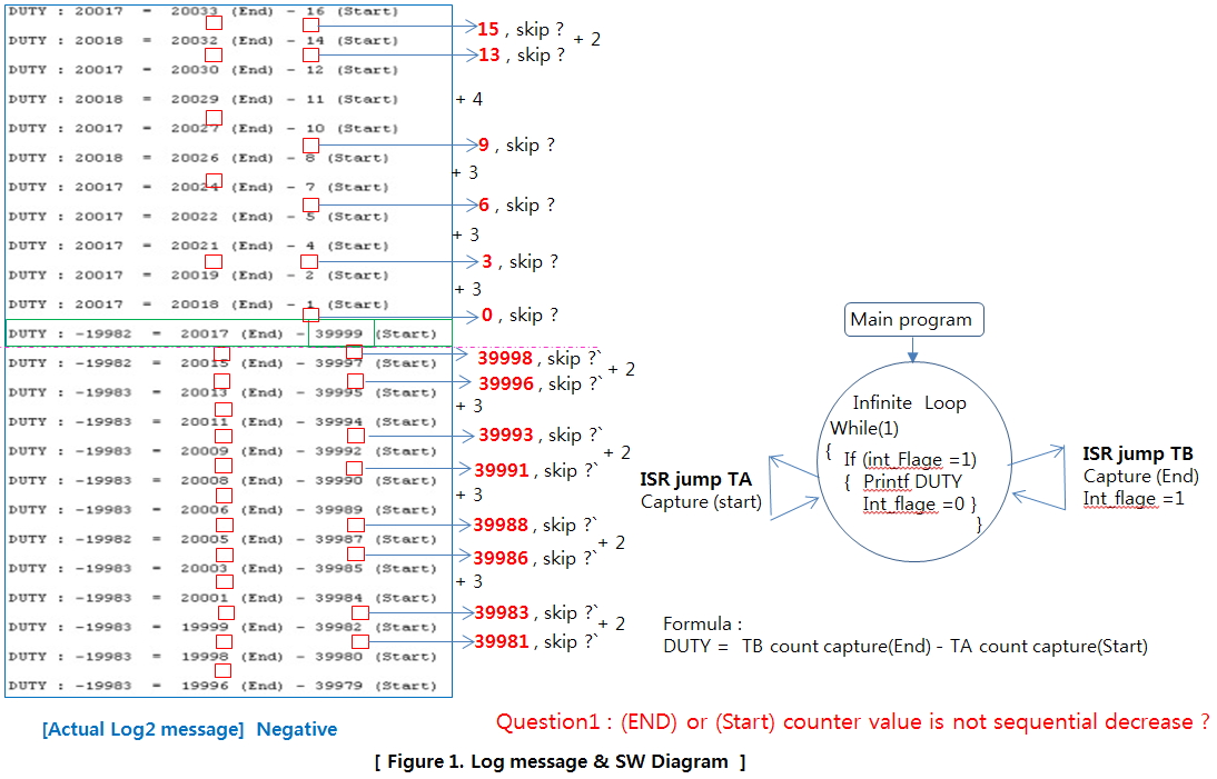
Hello
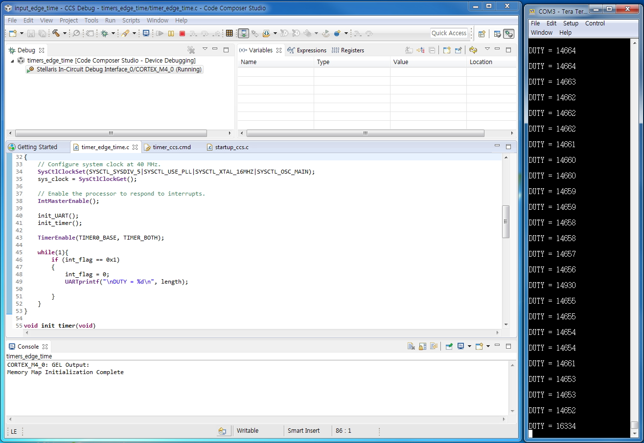
The input edge timer sample source code is required.
There is no example file in the Peripherals folder. ( edge_count, oneshot_16bit, periodic_16bit, pwm)
I need the edge_time example file.
thanks
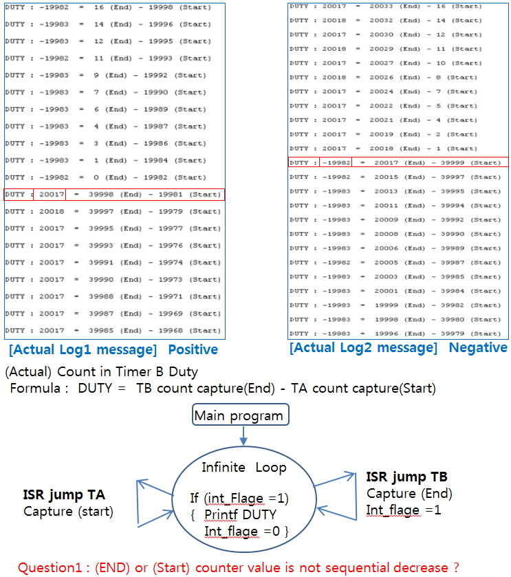
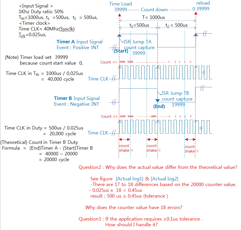
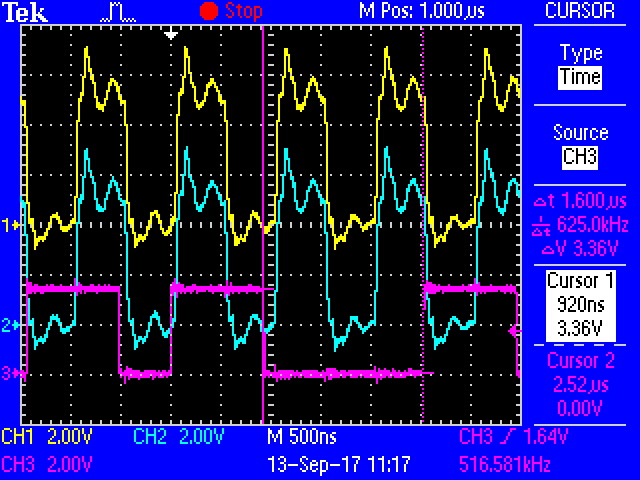
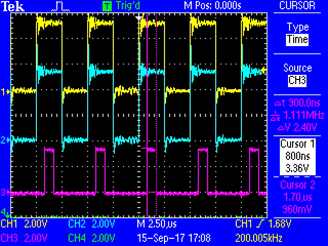
[Attach image of desired configuration ]

Hello
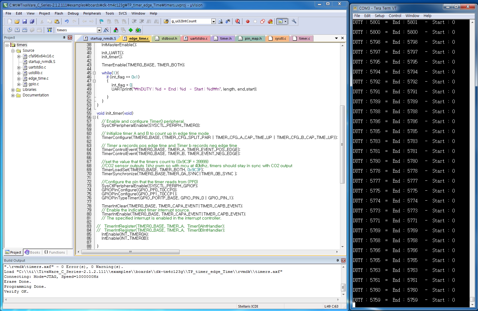
The input edge timer sample source code is required.
There is no example file in the Peripherals folder. ( edge_count, oneshot_16bit, periodic_16bit, pwm)
I need the edge_time example file.
thanks
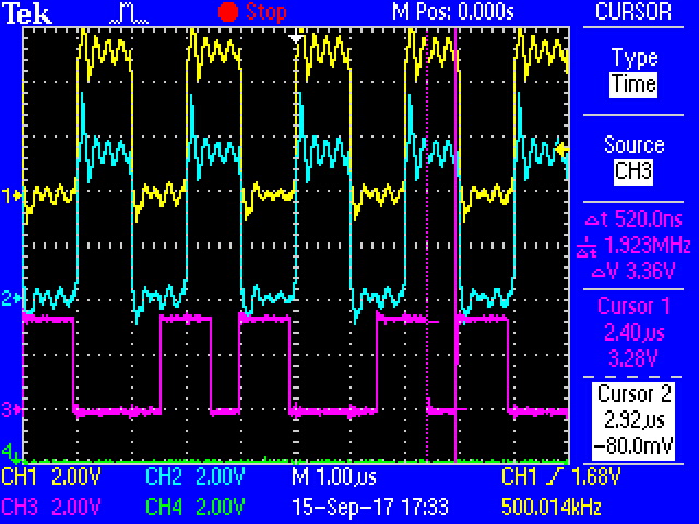
[Attach image of desired configuration ]