Other Parts Discussed in Thread: TM4C123GH6PZ
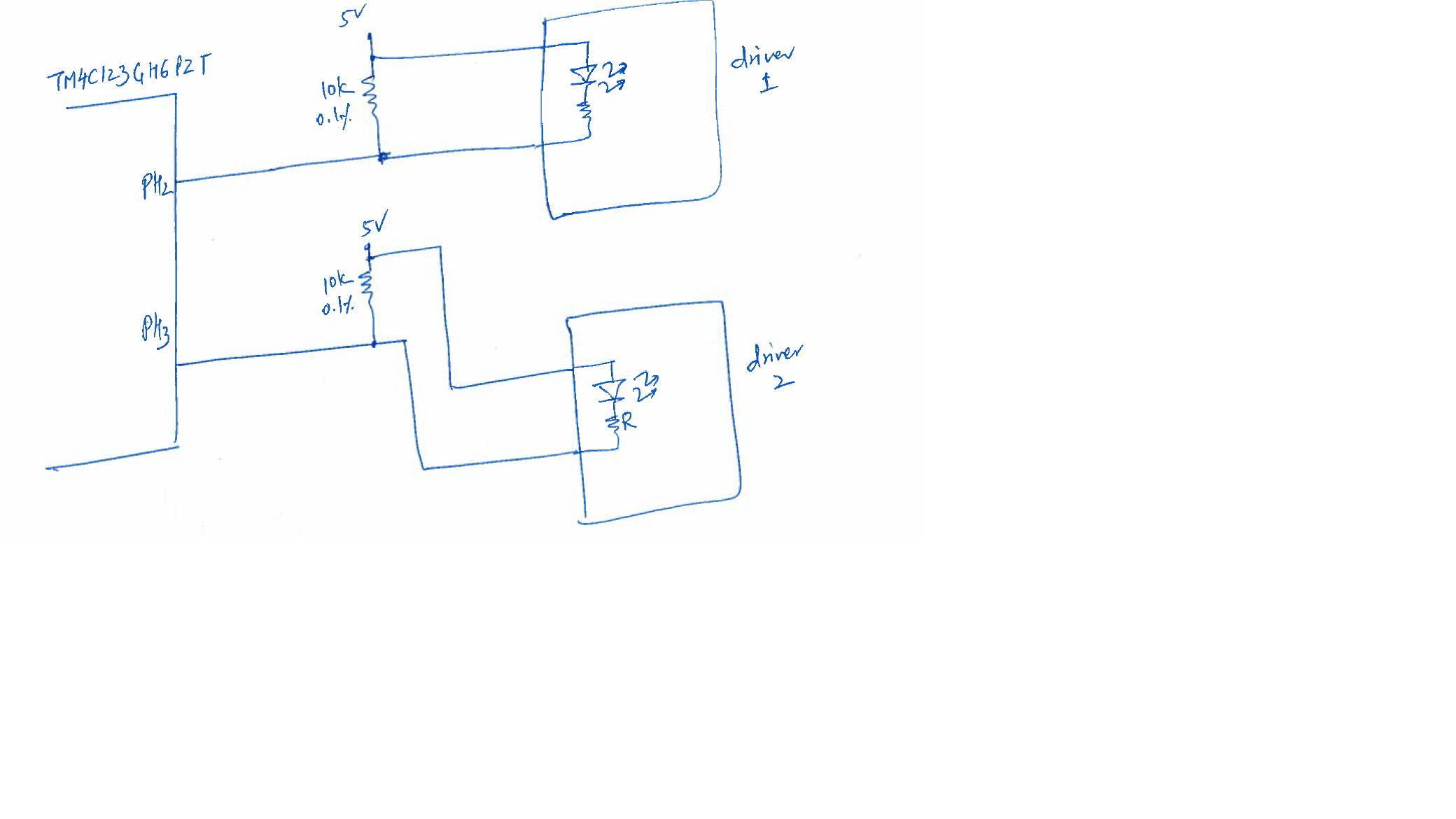
We have these pins driving opto isolator but with 18 mA drive. The opto isolators are used to drive stepper motor circuit. Both PH2 and PH3 pins are pulled high with 10K resistor.
We have about 50 boards build and running. Some of them are running for over an year.
On, working board, when I put a scope on connector that is connected to PH2 and turn the output off, I see 5V. And when I turn the output on, I see abt 440 mV. I measured the current sink by PH2 and it is abt 15 mA.
Recently two of our boards started exhibiting an issue. They would not move motor and hence I connected scope and I found that when the output is turned off in system, it would only go to 1.68V and when I turn on, it would reach 880 mV.
We replaced the board and motors started working ok. But since two boards in sequence failed, it prompted an analysis on our side. No visible damage on board (Checked under microscope). The continuity from pin to connector is ok. So the circuitry inside micro is damaged.
Is any body seen similar failure? Any probable cause?