This thread has been locked.

If you have a related question, please click the "Ask a related question" button in the top right corner. The newly created question will be automatically linked to this question.

TM4C1294NCZAD: ADC reading issue

Part Number: TM4C1294NCZAD
Other Parts Discussed in Thread: TM4C1294NCPDT

Hi,

I have a problem with ADC of TM4C1294NCZAD, the signal reading is dropped when I do more successive conversion ON ADC0 and ADC1.  Here is a description of the problem: 

when I’m reading +5V on AIN6.  I’m using both ADCs, and using the sequencers to read 8 channels on ADC0 and 7 channels on ADC1.  So far, so normal.

 Initially I had all the channels reading in order, so that AIN6 was the 7th input read by the sequencer on ADC0.  With this setup, the ADC reported the +5V supply was actually 4.12V.  I then tried moving AIN6 to be the 1st input read by the sequencer.  I then got it reported as 4.84V.

 I tried on another signal.  For the +3.3V supply, this was the 4th input read by the sequencer, and it reported 3.34V.  Moving it to be the 8th (last) input read by the sequencer, it reports 2.62V.

 Similarly, on the 12V signal is the 2nd input read by the sequencer, and reports 11.99V.  12V is the 3rd input read by the sequencer, and only reports 11.84V. This looks like a consistent problem with our ADC reads, where the first channels to be read are OK, and the more conversions we do in succession, the more the signal drops.

Could you please support me in finding a solution for this problem? 

Kind regards

Mourad

  • Hello Mourad,

    How are you managing signals such as 5V and 12V with the TM4C ADC? Do you have a voltage divider before hand to reduce the signal voltages to be at or under 3.3V?

    The maximum allowed voltage on the ADC pins is at the very most, 3.63V, with a typical max of 3.3V. From your description, you are sounding like you are inputting 5V and 12V signals straight into the device...
  • Hi Ralph,

    I am not putting these voltage straight into the device, you miss a bit because I have attached a copy of my schematic in PDF.

    I am using voltage divider for before Ti ADC:  5V and 3V3 I am dividing by 2 and for 12V I am dividing by 100k/22k which gives 2.16V as input to the MCU.

    Please find attached a copy of my schematic.

    Kind regards

    Mourad

  • Hello Mourad,

    Okay thank you, understood on the schematic now. I went ahead and deleted the schematic files from your post now that I have them downloaded. Let me review further.
  • Hi Mourad,

    We too noticed similar variance for same voltage measured by different sequencer steps of ADC0/1, even when the input divider follows design rules. Perhaps you can do a workaround in software to compensate for any step latency. Sequencer configuration might use IE on each step to avoid any unknown latency and further poll specific sequencers Trigger Processor in slower intervals via GPTM calls.  

  • Without viewing the schematic - it is (likely) that the voltage divider is causing an impedance 'mis-match' between the ADC's Input and the signal source.    The effect the poster notes - provides a 'strong clue' - that impedance mis-match has occurred...

    One effective cure - would see the voltage divider emplaced (instead) - at the input of a 'buffer amplifier' - in which the amplifier's (usually multi-channel outputs (4, for example) - provide a superior (lowered impedance) match to the MCU's requested ADC input impedance.     (while accommodating any  (possibly added) series (matching) resistance - and a low value bypass cap - which aids the MCU's ADC input circuitry...)

    Beyond that much improved, 'impedance matching' - the amplifier provides a necessary base for the creation of  various hardware, 'signal filtering' methods - (high/low/bandpass) - which complement (thus easing & enhancing) ... (any) software filtering efforts...

    As an "added bonus" - if you employ  'R to R'  (rail to rail) type amplifiers - and power them from the MCU's 3V3 - those amplifiers will (usually) provide a 'voltage limiting function' - preventing MCU damage thru 'over-drive!'     (Still - it proves wise - to limit the signal input to the amplifiers - to 3V3 - as well...)

  • Hello Mourad,

    As cb1 surmised even without viewing the schematic, your resistor divider values are very high and that is likely causing a lot of the trouble. To observe if there are improvements by addressing this, I would cut those values by a factor of 10 at minimum. Also the divider for 3.3V doesn't make a lot of sense, if the signal is 3.3V, why even divide it?

    Some background on how high input impedance can negatively affect ADC results in a sequence: e2e.ti.com/.../2512044 (The situations aren't identical, but the general reason behind why the problem occurs is the same).

  • Albeit Rs (source impedance) has not as much to do with the ground resistor in the divider and technically infers the upper R value in forward current flow into the cADC from the source. Technical seminars on SAR ADC point the lower R value in a divider is more a path out of the ANIx input for cADC switching noise sent to ground.

    Regarding provided link, though Bobs explanation makes sense it does not explain how the very same Rs divider (proper impedance) can produce different voltage readings relative to the specific sequencer steps. Either the step ANix Rs impedance is matching each steps TSN encoded hold time or it is not. It would seem from the perspective of sample hold times (TSN values in each step) could at times be slewing from outside signal noise! Hence a ferrite bead place in series with the ANix input signal seem to settle any ringing present in low amplitude analog signals.

  • Is it not (somewhat) 'poetic' - that one responder here - has a presently 'Open Posting' - admitting to being, 'Baffled why ANIx sample amplitude decreases.'

    Somehow it appears more productive to, 'Quench one's home fires first' - and only then (armed w/that victory/new knowledge - 'attempt to assist others...'

  • Hello Ralph,

    Thank you for help and support. Know I understand better the problem of impedance mis-match. I am still not clear one thing in datasheet, the ADC equivalent resistor  RADC 2.5KOhm and the RS Analog source is 500Ohm. If I reduce by 10 the voltage divider for 12V (100KOhm and 22KOhm), which gives 10K and 2.2K, the equivalent resistance 1.8KOhm, Do i need to be close in value to RS or to RADC?

    Do I need to added a 10pF cap as in nfigure 18-7 of datasheet? Thanks

    Kind regards

    Mourad

  • Hello Mourad,

    The issue with the impedance isn't so much trying to match it close to a certain value, but rather that there needs to be enough sample time for the voltage to stabilize on the sample capacitor. Therefore, the lower the source impedance, the better the ADC can perform measurements. If the design requires voltage dividers, low pass filters, etc. then either the source impedance needs to be kept low, and even then sometimes the sample time needs to increase to give the voltage more time to stabilize. This is why I suggested lower the values by 10x and see what improvements you see. There may be further tweaking needed depending on the result.

    Regarding the filter cap, the value needs to be considered along with Rs as it is intended to make a low pass filter. This can be done to keep high frequency signals (any signal more than half the sample rate) from being seen by the A/D input.
  • Well said Ralph.

    May I note - that across a 'wide range of ARM MCUs' (multiple vendors, Cortex M0 thru M7) the use of buffer amplifiers (even when configured as simple 'voltage-followers') has 'proven its worth' - time & again.    (greatly lowers impedance while  'adding much beneficial design capability & flexibility!')

    As earlier stated - the 'lower end' of such buffer (op-amps) may include 'Quad Devices' (4 channels) simplifying board layout while reducing cost.

    If  'cost alone' is the objective - it IS possible - to design the pcb such that these 'buffer amps' may be (selectively) 'fitted' (i.e. even NOT fitted) via the addition of strategic jumper (links)...

    It proves HUGELY EXPENSIVE to 'trash a design' - due to 'impaired/inconsistent performance' - when such a (relatively) low cost 'insurance policy' (buffer amps) - stand at the ready!    (even when such amps were 'un-noted/rejected' - especially when amps were 'un-noted/rejected!')

  • Another reality check reveals SAR successive approximation register is just that, not an exact measure no matter what the Rs impedance is made. Often with trashy signals the Rs value might require higher impedance to get a stable reading when other frequency/s could roll around in the desired approximation sample. Hence TDK/other vendors ferrite beads <0.10$ placed in series with approximation analog signal is also a great low cost addition.  

    Perhaps CB1 can enlighten us how the buffers output is configured for an external discharge cap or series R value. Transient analysis of such buffer would be beneficial in that endeavor.

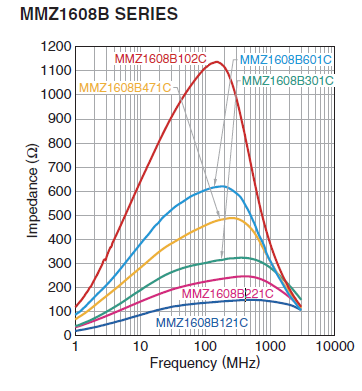
    MMZ1608 is just recently proving a good investment in our design, just wish we had put them in more places versus 0402 0R. Yet MMZ sits nicely atop 0402 pads with only marginal hangover. So far we have tested the B121C and good results were noted (samples) places where 0R were series to 3v3 LDO +5v inputs for one. The higher impedance B102C/B601C are now on order.

    B material: This type is perfectly suited for fast digital signals. By equalizing R components and X components that beads possess at a frequency of 5MHz, it is able to suppress overshooting, undershooting and ringing of fast digital signals.

  • cb1_mobile said:
    Is it not (somewhat) 'poetic' - that one responder here - has a presently 'Open Posting' - admitting to being, 'Baffled why ANIx sample amplitude decreases.'

    Exactly revealed by forum members SysCtlClockFreqSet() incorrectly configures PLL making VCO 240mHz instead of an expected 480mHz. Also the primary cause of impedance mismatch in the divided ADC clock rate as most were factoring impedance for 2MSPS and actually only getting 1MSPS or 500KSPS with ADCCLK being 8mHz versus 16 or 32mHz. We were puzzled how Tina transient analysis of the Rs impedance circuit could be so far off on the bench time after time. That's called excellent issue collaboration!

  • Not quite mon (baffled) ami.

    The misstated VCO frequency (may) explain the introduction of measurement errors - but appears not to 'fully/properly' explain, 'YOUR bafflement at 'sample amplitude DECREASE' - ALONE!

  • It was missing so many samples as the PWM duty cycle increased the acquisition point was changing and the amplitude dropped off. But it was much more since the impedance was also inflicting the frequency roll off the entire analog sample was so messed up!
  • Well - for everyone's sake - let's hope that this 'new insight' leads to improved (and lasting) MCU performance - and that ALL Users benefit...

    Thanks to all vendor staffers - for aiding users (and we 'User-Specifiers') - who receive heavy, 'canon-fire'  when devices we specify for (multiple) client adoption, 'Fail to perform to Spec.'

  • Yet later questions of 30Mhz ADC clock being actual speed and 60Mhz likely required for 2MSPS. Seemingly more obvious relative to USSB0 480Mhz PLL speed requiring VCO 480Mhz not working with VCO 240Mhz configuration. Same VCO for USB0 shown main clock tree used for ADC clock, forum believed required VCO 240Mhz/8 for 30Mhz or 2MSPS.

    A 60Mhz ADC clock seems required for 2MSPS, datasheet perhaps misprints 32Mhz! It don't seem to be overclocking ADC module since CPU temperature is not going higher as result of double ADC clock speed. Seemingly ADC0 temp sensor would get hotter if the modules FIFO's were being over clocked.

    So the question 30 or 60Mhz relative to lasting performance may simply be datasheet misprint.

  • Obviously was confused by past TI gurus not taking time to investigate why USB0 device mode was randomly disconnecting Windows device client, reported issue this forum 2015, again 2018.

    One word fits the case, e.g. Bamboozled!
  • Some here (I am told) suggest that 'you' ... Sharpen & READY - your (well exercised) - 'CROSS OUT Pen...

  • Redacted facts based on false truths leaves gut feeling oddly ill or is that just the morning dew barking. 

  • How low is low in the TI hand book of source impedance doctrine. Could my low be even more low than TI's typical ideal low and how low is that low? TI Tina DC analysis would have one believe negative Rs impedance is lower than being simply low. Yet AC analysis mocks those highly negative values , being positive Rs Impedance can be low but not lower than negative low.

    Perhaps AC rms Rs impedance more closely reflects an analog signals frequency impedance, also being low relative to TSN hold values? So negative values are lower than the lowest TSN hold time 0x0 encoding , lowest low possible in a low perspective. So a negative Rs impedance is the absence of any resistance or a void in space time, since 0 ohms was always the lowest low one could ever expect infinity to be at any given time of any source impedance.
  • It (remains) suspected that the 'simple - almost painless insertion of an op-amp' - would provide beneficial to your 'higher voltage' (yet suitably reduced/divided) voltages - as presented to the MCU's ADC.    Higher voltage op-amps are available - and their accommodation of that 'higher voltage' may work to your aid.    (added low-pass filtering is one consequence - usually brought on - by  'higher voltage accepting' - op-amps...)

    Continued resistance to such suggestion may (insure) your thread grows ... (even) deeper roots.     (and we are told - those 'roots' (already) have displaced (many) of your destroyed Power FETs - now once again 'enjoying the light of day' - having 'escaped' their sodden burial ground...)

    It is likely that you must still resistively divide your higher voltage - prior to presentation to the op-amp - and (then) thru to the ADC.

  • If only the ADC sample rate was true as posted stressed acquisition times properly fulfilled, speaking in past tense of course. No FETS lost after TM4C1294NCPDT driving HV inverter 2016 on, high lights something wonderful is going to happen.