This thread has been locked.

If you have a related question, please click the "Ask a related question" button in the top right corner. The newly created question will be automatically linked to this question.

TM4C1294KCPDT: ADC0 acquisition compatibility

Guru 56043 points
Part Number: TM4C1294KCPDT
Other Parts Discussed in Thread: INA240, REF2033, LM94022

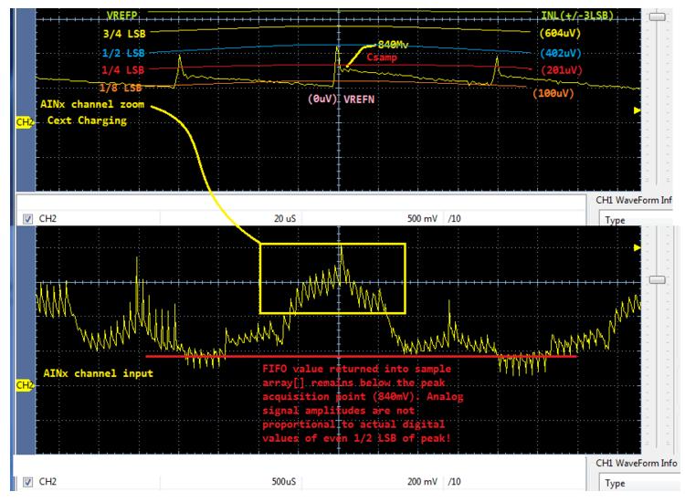
Why is TM4C1294 SAR unable to follow this signal to scale or equal vertical voltage ramp (elevation) since INA240 output was developed to work with SAR ADC?

After more testing of signal via several different analog pulse profiles again only reveals TM41294 ADC can not lock onto the top acquisition points to create a monotonic rise digital representation of current rising. The SAR embedded in MCU always chooses to acquisition the pulsing signal near the horizontal center and mostly produces bloated representations of the original signal.

It appears there is an issue with ADC to properly sample a ramping vertical growing signal in order to build stepping monotonic linear digital values (rise/fall) from a pulsing signal. All the Rs impedance rules followed yet ADC can not acquisition from the top of full scale (VREP) down or even the bottom (VREFN) up. Sure if we stick pure DC current into AINx channel CADC will stay charged during Cext recovery periods so 475nf Cext shown below (Table1) is a band aid to being with. The INA open loop gain into ANIx is not being properly handled by ADC0 for what ever reasons.  We need to figure out what and why then get it fixed like any other engine, when it fails we take it to a mechanic to fix it, do we not?

Otherwise the entire INA current monitor narrative has been falsified upon the community suggesting any SAR ADC can produce digital integer representations of current (values) from a ramping analog signal without SW trickery being involved. I truly do not want to believe such occurs at TI and they make every best effort to ensure all SAR devices are compatible with a flagship device. Seemingly there is something wrong with the TM4C1294 SAR ADC not being able to correctly interface (ASIS) with the very same companies current monitor. Might something have been left out of the picture a customer might require to make a proper judgment call? Perhaps similar testing INA240 experimental PCB in the LAB with EK-TM4C294XL will verify this conversion thread has merit?

That said, once again why would the ADC not be able to properly acquisition the signal below, what is wrong with it? What attributes must pulsing signal have for proper acquisition to achieve at least 1/2 LSB resolution (microvolt) or even 1/4 LSB near (Csamp) being industry typical SAR acquisition standard? Is it possible TM4C1294 ADC may not properly work with INA240? Why would TI not test the INA240 on several different MCU to ensure it being fully SAR compatible with PWM intended modulation? Why would TI expect the customer to modify the INA240 output to work with TM4C1294 SAR and not notify the community of such an expectation even in WiKi documents? 

Point is these questions indicate some kind of ADC anomaly must have flown under TI radar screen. The INA240 should not be any problem for TM4C1294 SAR to reproduce the intended digital results from an similar frequency periodic analog input signal.

  • Table 1 shows settling times for different types of ADCs versus source impedance. To use this table, find your ADC in the first three columns based on data sheet specs. Secondly, if you use an external capacitor, Cext, make sure it is as big as the one listed in the fourth column after accounting for tolerance and aging. If your Cext is larger than the one listed, it will affect the result-columns favorably if at all.

    Calculated Cext value (475n/0.475uf) while our Cext 22n (capture above post) has already pushed INA240 amplifier open loop gain (peaks) well above typical. Part of the peaks occur after filtering large EMI the 240 allowed in through the non-metallic plastic case.  Yet another hurtle the INA group asleep at the wheel, developing devices with less than proper shielding for a PWM environment that interface with SAR ADC is simply poor engineering at best. Still as stated no reasonable value of Cext or Rs makes the TM4C SAR able to properly decode the INA240 analog output into a digital format VREFP-VREFN.  

    10 Consequences of Inadequate Settling Time
    If Cext is at least as large as what is shown in Table 1, then the maximum time to settle Csamp is less than 130 nS, which is very small. There should never be a need to cheat on this parameter.
    The only time it makes sense to omit Cext is when Rsource is very low, otherwise, the channel will be sensitive to noise. Generally, Rsource is low only with sensors that have outputs driven by opamps. In thiscase, Rsource is < 100 Ω and still there is no need to cheat on settling time. Inadequate settling time leads to crosstalk. As discussed at the beginning, this is charge transferred from one channel to the next and accumulated on Cext over many conversion cycles. With crosstalk, each channel disturbs the next channel in the group to be converted. This phenomenon is due to the residue of charge on Csamp after converting channel[N] which contaminates the charge on Cext[X+1] of channel[X+1]. very good rule is don’t cheat on Settling Time.

    11 Consequences of High-Source Impedance
    If Rsource is too high for the desired conversion time, the only consequence is a time lag in the response of the channel. Full ½ LSB accuracy will occur, but it will be delayed according to Equation 18 and
    Equation 19. If Cext is not present or if it is too small and you have cheated on Settling Time, then results will be inaccurate, there will be crosstalk, and full ½ LSB will never occur.

    13 Conclusions
    Unbuffered multiplexed ratiometric ADCs are excellent in terms of cost and producibility, but careful consideration must be used in designing with them in order to obtain the expected results.

    Most notable are the following points:

    • Settling Time issues can be easily diagnosed by examining the waveforms at the ADIN[X] pins while the ADC is running in a continuous loop.
    • In most cases, the best speed/impedance results will be obtained by including Cext if the proper value is selected.
    • Given a specified number of bits of resolution, the proper value of Cext can be calculated independent of frequency and source impedance.
    • Never cheat on Settling Time. It will only get you unpredictable results!

  • BP101,

    I am not sure I understand your point. If you are not getting the expected results, but you have designed for sufficient settling time, then the problem is somewhere else.

    What is the maximum value you sampled? What is your sample rate? Remember that at 3.3V reference, one LSB is 0.8mV. Are you using an external reference or an internal reference? Then maximum total error for an unadjusted internal reference is +/- 30 lsb or 24mV.

  • Hello Bob, :-)

    Bob Crosby said:
    I am not sure I understand your point.

    The point is the TM4C can not lock on to the acquisition points (Csamp) shown in capture nor produce a scaled LSB to MSB representation of the analog voltage as it rises to any peak under 3.1v full scale. Even if we bias the 240 output (1.65v) ADC can not sample those same acquisition points into a scaled solution that represents the digital current measured in two ways. First by digital readout, 2nd by GUI scope widget with rising slope. This issue can't be the result of +/-30.0 LSB error since converter does produce a copy of the original input signal though greatly reduced in scale. The odd part is PWM duty cycle produces ratchet steps for the ADC not locking onto rising slow peaks above the last acquisition point in order to form a monotonic increase in amplitude. That seems to infer Charge sharing is being dumped after each conversion. Hercules has a register to force that very dump. 

    Bob Crosby said:
    Remember that at 3.3V reference, one LSB is 0.8mV. Are you using an external reference or an internal reference?

    Tried both REF2033 being far to noisy, currently using internal VREF. Anyway SAR acquisition conversion is detected in microvolts not millivolts. So Figure 15-9 first vertical mark 1/4 VREF 825mv, everything to the left of that 1st mark 825mv down to 0mv being 0LSB. That 1/4 VREF is the converters digital output scale, not sample scale (microvolts) relative to each acquisition point inside our full scale. That is why all the graphs in Hercules PDF indicate (uV) on the left side to explain 1/4 LSB resolution is very fine. Acquisition 1/4 LSB resolution occurs as seen by the analog side of converter during sampling, not the AINx analog channel voltage or the VREF (millivolt) digital scale. Hercules PDF shows us sampling happens in much smaller baby steps of the converter not directly related to VREFP-N, fact the TM4C1294 datasheet seems to omit.

    It seems TM4C SAR the entire analog signal is being directly passed into the converter and only scaled down (compressed) relative to REF and not being acquisitioned relative to VREFP in full scale of Fig15-9. Seemingly that is why there is no top/bottom point of reference for digital output relative to VREF for a single ended channel input when the analog signal has fast periodic rise/fall times. Now if we rectify that same signal it may very well properly acquisition the slower rise times. Table 1 shows our signal is settling a bit slower but there is plenty of slew in the signal up to 80us for Cext charge sharing with CADC.

  • It is usual - when presenting (another's) data - to provide attribution. Forcing your readers to 'guess' your source ('Hercules' and (some) extract from 'INA240') - as well as your 'intent' (what should be gleaned from such an 'undescribed Data Dump') proves confounding & off-putting to your readers.

    It is not especially productive to (always) violate 'convention.'
  • Oddly Figure 15-7 shows us 1/4 VREFP-VREFN from the top of full scale down. Yet that same scale of digital markers is not present in the converters results into the hardware averaging engine nor are they present in the FIFO data read back into an array[]. Seemingly even the analog linear sampled voltages digital converter has opposite reference VERFN-VREFP.

    Fig 15-7
    BTW: mV per ADC code = (VREFP - VREFN) / 4096 and 1/4 VREFP-VREFN or 825mv/4096=201uV 1/4 full scale

  • That is why the link exist to past threads top most post. If you check above there be table 1 (input referred) + few notes. Table is not specifically relative Hercules SAR but includes different SAR's 10bit 12bit needed to determine proper Cext.

    Again the focus being relative to TM4C1294 ADC incorrect acquisition of the signal posted. The mere fact signal was named from the source from which it came is a bonus!
  • Both the 'drawings' and 'method' presented here - appear to me - 'outside' normal/customary  'ADC Evaluation Techniques.'

    I (remain) unclear as to the 'true source' of (both) the 'Scope-Cap-Like' images - earlier presented.    Please (accept) that if you've (briefly & earlier) described the 'creation of these images' - there exist (now) 3 separate threads - all focused upon this issue!      (forcing such a 'labor intensive search' upon your 'would-be' helpers - proves not to your 'best interest.' )   

    For clarity - I've copied them (from the initial post - this thread) - and present  here.

    Now - I (suspect) but do not 'know' - if these images are 'True Scope Caps' - and even if (having started as such) they have not gone thru (some form) of post-processing and/or manipulation.    Might you detail?

    What I believe to be (very) 'Missing' - is the, 'Pure (unmodified/processed Scope-Cap of the 'Test Analog Signal' - captured as close as possible to the MCU's ADC pin - and w/scope Probe's GND Lead removed!   (I will illustrate the proper means to conduct such 'Probe Modification' later - w/in this post.)

    BP101 said:
    Why would TI not test the INA240 on several different MCU to ensure it being fully SAR compatible with PWM intended modulation?

    You have asked, 'Why this vendor has not, 'Had the wisdom - to fully/properly (and exhaustively) ANTICIPATE your SPECIFIC USE CASE - in their 'Automated Testing' of the MCU's ADC!'    Having past 'managed' at a similar Semi-Giant - I can report that, 'They too - made NO SUCH Anticipation!    Have you NOT opened a 'Pandora's Box' - of, 'Testing EVERY IC' - in combination with 'EVERY OTHER IC' - Ever Created?    

    I suspect that you (may) secure the 'Greatest Probability' of  (even further) Vendor Involvement/Guidance - by replacing the INA device with a properly designed & implemented (far more general) 'Analog Signal Source' - capturing the input Analog signal (presented to the MCU)  'properly' - minus Gnd probe lead - and presenting your ADC's resultant 'capture' of a sufficient number of analog conversions.     (sufficient to enable (proper) Compare/Contrast of the "Analog Input Signal" impressed - versus the ADC's Conversion Results.)    

    This vendor has 'LONG been noted for providing (particularly) intense Tech Support to you personally' - restricting their, 'Standard ADC Test Procedure' - to YOUR 'HIGHLY Unique Demands' - may be seen by (some) as 'unreasonable.'  

    Proper Scope Probe Technique:

  • Hi Bob,

    Bob Crosby said:
    If you are not getting the expected results, but you have designed for sufficient settling time, then the problem is somewhere else.

    Agree and that is why this thread is ongoing until the nitty gritty of the issue is resolved. Likewise 475n Cext would push INA240 open loop gain into extremely higher error %, more than it is already by the distorted gain peaks in capture. The 22n Cext of posted capture shows us settling time is not causing the SAR to drop shared or CADC charge hold. Seemingly the ADC converter is not moving LSB bits into MSB circular positions after each cycle group (80us) required to elevate digital results relative VREFP 3v3 full scale of the analog signal.

    Even if there was 30% error, the missing left shift of FIFO bits on the digital side of converter still fails and instead dumps VREFP samples all the way down to VREFN each cycle group time.  Seemingly that is not correct SAR converter behavior even if channel cross talk was in the mix. Perhaps this also explains why pure analog DC signals digital array[] 10ths position (mV) hunts cycles at high speed 0-9 never to fully stabilize 2x averaging. The SAR converter seems to dump CADC charge to ground each cycle group time during Cext recovery period no matter if NSH matches Rs impedance. 

    Have to wonder at this point if perhaps hardware averaging adds some kind of errata upon converter, e.g. FIFO not properly left shifting LSB results into MSB bit positions after each cycle group time? That necessary shifting only seems to occur if the analog voltage side of ANIx spikes very high but only for 1-2 cycle groups of acquisition does that left shift occur. So the circular FIFO is not acting circular as it relates to the converter handshake of LSB into MSB cycle times, hardware averaging or otherwise being functional at all for any A/D conversions. 

    I updated the signal capture 1st post to indicate what the analog converter sees each 80us group time. I realize microvolt acquisition is very different from Fig.15.9 (generic) presenting only the millivolts scale from a digital results perspective 0-4096.  Yet that is not how the SAR converter acquisitions in ratios (1000:1) in the 3v3 VREFP digital perspective of analog settling being correct.

  • CB1 where do you come up with nonsense capture is not real and then repost the updated capture from 1st post above. Extending thread length into multiple pages is not desired nor warranted. I think by now INA signal is not the issue, rather why does the TM4C1294 ADC not properly handle similar periodic signals with hardware averaging enabled or not. My point was the LSB values as explained to Bob in last post are not left shifting into MSB as rapidly they should.

    Good example of errata; Two LM94022 sensors after POR, ADC1 SS1 starts sampling via trigger processor 1 second intervals. It takes 6 GPTM seconds for the two sensors with 32x hardware averaging to reach ambient steady state PCB temperature. Say we trigger SS1 via PWM0, it still takes several seconds for the FIFO to return correct values. Both sensors have no Cext and have 3K9 pull downs. Are we cheating on Cext, perhaps not as 1000n Cext received cross talk from PWM activity on both sensors. It is possible some PWM cross talk but it is not showing on the signal above since it is in the same 80us time domain and that is considered acceptable, e.g not cross talk.

    Please try to focused on posted issue of SAR not properly moving LSB digital values into MSB bit positions of previously settled group times via CADC charge NSH hold times. The fact INA signal was to allow vendor to test for themselves how bad the issue is when it should not be at all. Again tip of the iceberg for the digital converter is not behaving even with pure linear analog signals. We can not get clean millivolt stability in the 10s place holder, result of digital converter failure and hardware averaging barley makes a dent. If Cext was made 475n the PWM inverter would easily lock the MCU up making it useless.

    Captured signal (no matter quality) is only active in the same time domain as PWM activity. That makes ADC settling of group times follow 80us PWM periods. That is also when digital converter fails to left shift last LSB bits into next higher MSB so positive sample stepping relative to VREFP can occur. The FIFO value multiplied by the PWM modules duty cycle corrects digital converters acquisition break down. Converter fails to << LSB into higher FIFO bit cells and stalls rather than incrementally ratcheting up to the next analog voltage level when being settled to (3v3 - 1/2 LSB). 
     
    The definition of settled signal:
    The object is to get Csamp charged to within ½ LSB of 3.3 V before declaring Csamp settled.
    As the knee rises above the [3.3 V - ½ LSB] line with increasing Cext, there is a rapid reduction in time required for Csamp to settle since being within ½ LSB of the 3.3 V line is the definition of settled.

  • Bob Crosby said:
    What is your sample rate?

    The ADC clock is set for 30MHz 2MSPS and behaved the same 16Mhz ADC clock. Circular FIFO must keep pace with digital converter << LSB bits into MSB bit positions.

    Logically serial FIFO clocking requires 16x ADC clock 30MHz order to maintain synchronous pace with digital converters acquisitions (2MSPS), that logic requires PLL=480MHz. This is a conundrum as MOSC=25MHz and PSYDIV +N pre-divides PLL block 240MHz, according to recent discussions of PLL block issues.

    Like wise 16MHz ADC clock (1MSPS) rate the required FIFO serial clock 256MHz actual VCO speed falls below the synchronous speed of digital converter, so we had same failing conversions. We would settle for conversion results from PLL=480MHz and the FIFO serial clock rate of ADC0/1 modules clock being 30MHz .   

    This issue was a gut feeling after Charles recently discovered PLL block VCO was running half speed. Sure seems clocking could be the fish that got away last year, now with a hook in its mouth. At least clocking is an avenue to try and make some changes so the FIFO speed matches the converters clock rate of 30MHZ.

    How can ADC0 FIFO serial clock be changed from 240MHz for it run at full speed of 480MHz and keep synchronous to the digital converter?

  • May I (repeat) my earlier question (unanswered, above)?     "Now - I (suspect) but do not 'know' - if these images are 'True Scope Caps' - and even if (having started as such) they have not gone thru (some form) of post-processing and/or manipulation."    Might you (STILL) detail?

    Your (assignment) of 'nonsense' to that question - in no way explains nor details - thus proves (both) ineffective & unfriendly.    (Note: I took pains to, 'formulate that sentence' - as I believe the response (may) prove useful.)

    It is believed that 'yours' are the first such, 'Presentation of such issue.'     And - as you report 'issue' - the completeness of your report (to include input signal waveform - (as best as you can achieve)) is deemed as, 'normal/customary' - and (surely) required during  standard ADC 'test/verification.'

    BP101 said:
    ... and then repost the updated capture from 1st post above.

    I did that to, 'Save Wear & Tear' upon your Helpers!      Your 'issue' may be of HIGH concern/focus to you - yet surely of (somewhat) lesser focus - to your 'helper crüe.'      Anything to 'Ease the job of your helpers'  (one would hope)  would  'warrant your approval.'    While we, 'Feel your (ongoing) pain' - placing 'roadblocks' (repeated searching/scrolling) in your helpers' path - proves not to your advantage!

    BP101 said:
    Captured (ADC) signal (no matter quality) is only active in the same time domain as PWM activity.

    It is noted that you (usually) introduce 'MANY FACTORS' into your 'Forum Help Requests.'     As you know - 'KISS' directs the, 'Severe Reduction of such 'Multiple Factors!'     Minus a, (proper) 'Limited, Linear Progression Path' (only proceeding upon 'Measured & Confirmed (INDIVIDUAL ITEM) Success') - both the clarity & speed of  Diagnosis - are impeded...

    BP101 said:
    ... ADC settling of group times follow 80us PWM periods. That is also when digital converter fails to left shift last LSB bits into next higher MSB so positive sample stepping relative to VREFP can occur.

    Has (this) not strayed from 'Real Confirmed Measurement' - into 'personal opinion?'    How have you reached such conclusion?    If this has been 'measured' - your detailing the (mechanics) of such measurement - are sure to, 'Build your case.'    (a 'blind defense' - minus tech detail - Not so much!)

    There (still) remains a (rather large) elephant - w/in this (notably  tiny) 'Settling Signal Room.'     Your goal (not all here may know and/or recall) is the full-proper control of a rather large BLDC Motor.   (of your own design & development - which my group has (always) admired & respected.)

    My group - having (quite profitably) 'Designed, Built & Shipped' many hundreds of such 'BLDC Controllers' - believe this 'Settling Signal' issue to either: 

    a)   Not prove of 'significant and/or disturbing' impact
    or
    b)   Not to have occurred

    Any such 'Mixed Signal Device's ADC' (i.e. any MCU) cannot be expected to equal the performance of 'Dedicated Component ADCs.'      AND - with my firm's development of  'MOTOR-CURRENT, TREND RECOGNITION' - our group (perhaps blindly) has (ESCAPED) any such, 'Settling Signal Upset!'

  • The post was unnecessarily updated with the very same capture again, what was the purpose to do that on this same post. Please kindly remove second capture as it came after I had just updated this post. Simple scroll up page now to difficult for readers? The capture of signal is 1000 samples deep and very real.

    Getting to the nitty gritty should be fast and furious not require so much mustard on the dog so to say. There is no personal opinion when the data being returned from the converter is not the ADC sampled acquisition points are documented as being theory. Either the SAR is working properly or it is not, in this case it is not!

    The captured signal artifacts of Cext charge sharing groups are theory, 1/2,1/4,1/8 may not be exact scale but the point made is obvious! We don't need to dig any deeper on the AINx input signal as NO filtering changes of INA output has produced the expected behavior of TM4C1294 SAR. Your combat ready boots have seemingly forgotten the INA output was designed for typical SAR acquisitions, e.g. properly timed SAR acquisitions, not unsynchronized babble of a misbehaved converter clocking incorrect FIFO data.

    It is painfully obvious that ADC clocking some how misaligns converter data in FIFO being input from the INA complex wave form and can not manage the signal fed into it with typical RS impedance or Cext per Table 1. Note the signal 80us period is still considered settled under green rectangle of table 1 above.

  • cb1_mobile said:
    Has (this) not strayed from 'Real Confirmed Measurement' - into 'personal opinion?'    How have you reached such conclusion?    If this has been 'measured' - your detailing the (mechanics) of such measurement - are sure to, 'Build your case.'    (a 'blind defense' - minus tech detail - Not so much!)

    Several times have stated the digital readout stays flat does not increment perhaps 100mA above the set minimum derived value from the FIFO. Again the GUI scope widget trace only widens as scaled down compressed analog signal, it does not rise in amps scale as predictable theory states it should. All that changes when the FIFO results are multiplied by the PWM duty cycle to produce ratio metric monotonic SLOPE in the current reading from FIFO. 

    Instead of going to war how about look into why the clock rate on the FIFO is not keeping synchronous with the digital converter. Oh that's right the datasheet conveniently removed all ADC clock inputs from figure 15-2 and main clock tree Fig.5-5 not much use either to determine how to pipe 480MHz PLL/VCO into the FIFO serial dot clock. 30Mhz is not enough bandwidth to synchronize the converter to the FIFO and maintain nanosecond acquisition based on nanosecond settling times. Anyone who thinks 30 MHz alone can fulfill that requirement is selling snake oil.