This thread has been locked.

If you have a related question, please click the "Ask a related question" button in the top right corner. The newly created question will be automatically linked to this question.

TM4C1294KCPDT: ADC0 FIFO clocking

Guru 56043 points
Part Number: TM4C1294KCPDT
Other Parts Discussed in Thread: EK-TM4C1294XL, INA240, INA282

It would seem to properly distribute AD converters settled acquisitions synchronously into serial FIFO in real time the FIFO clock must be running 16x the 2MSPS rate of digital converter or 480MHz.

The ADC modules main clock tree seems to indicate the analog divided clock (32MHz) occurs after [%N] block yet the 480MHz VCO should also pass through it into the blue box for the FIFO serializer. 

Dividing PLL (480/2) our VCO runs 240MHz and fails to satisfy circular FIFO synchronization << LSB bits into (ratio metric) MSB bit positions as real time settled acquisitions occur in the converter for even slow periodic signals. Effectively ADC clocking issue manifests into real time signal acquisitions being out of synchronization with the application attempting to process questionable FIFO data. In certain cases depending on the analog signal being periodic or mostly linear the condition procures samples with either large error INL >3% or even mostly distorted samples.

How can we get the VCO to produce 480MHz for the ADCCLK  (blue box) when SysCtrlClockFreqSet() is currently pre-dividing PLL/VCO 240MHz?  It would seem ADC clock being recent discovered issue has tentacles reaching beyond simply the ADC clock divisor. The datasheet diagrams and text are both vague on exactly how said ADC clock is being distributed and specifically divided as it relates to Fig.15-2 individual blocks. It would seem diagram below leaves open possibility ADCCLK could require 480Mhz to satisfy FIFO << LSB bits into MSB cells so SAR ratio metric behavior occurs for all signals being converted and not just slower steady state signals. Something is not right in how ADC0/1 are behaving with even slow periodic signals. It only compresses periodic single ended analog channel samples into scaled replica of the original periodic signal, that is not the behavior always desired.

  • The shift register (I would not call it a FIFO) of the successive approximation register (SAR) analog to digital converter is clocked by the ADC clock which is specified as a maximum of 32MHz. It can be derived from a divide down of the PLL VCO output. 2MSPS x 16 = 32MHz (not sure why you think the ADC serializer must be clocked directly from 480MHz.

    That being said, there is a known erratum on the TM4C129 devices (SYSCTL#22) that the output divider of the PLL used to generate the system clock may not get properly loaded leaving it at divide by 2. The workaround in the latest versions of TivaWare use VCO = 240MHz for a 120MHz system clock even if SYSCTL_CFG_VCO_480 is used in the function SysCtlClockFreqSet(). Use the function SysCtlVCOGet() to determine the actual VCO frequency that was configured. With a 240MHz VCO the maximum ADC clock you can use is 30MHz (not 32MHz).

    Is the sample rate the issue you are having? You did not answer the question I asked in your previous posts, 1) what sample rate are you using? 2) what are are the values you are getting from the ADC? and 3) What are the values you are expecting?
  • Hi Bob,

    Bob Crosby said:
    It can be derived from a divide down of the PLL VCO output. 2MSPS x 16 = 32MHz (not sure why you think the ADC serializer must be clocked directly from 480MHz.

    Well for one that is typical for UART FIFO serial data transfers in asynchronous communications. Have determined VCO speed was being divided in half by later version of Tivaware but we were still using older version SysCtlClkFreqSet() which correctly set the PSYSDIV N3+1 for the SYSCLK divisor. We had set the ADCCLK divisor believing VCO actually defaulted to 240MHz as no matter PSYSDIV value. VCO was not 240MHz either Tivaware version, actually VCO=536MHz launch pad testing. The testing I did the other day to achieve positive scale gain, ADC clock was running 60MHz and was likely skipping over AQ points. Note the SYSCLK was 120MHz in older version and 60MHz with latest Tivaware code, seems to be setting PSYSDIV incorrectly. Now we will set ADCCLK/17 (31.7MHz) to trim for over clocked VCO.   That is if SysCtlVCOGet() actually reading speed correctly. It required an array[0] to capture the callback contents as integer value.

    Bob Crosby said:
    Is the sample rate the issue you are having? You did not answer the question I asked in your previous posts, 1) what sample rate are you using? 2) what are are the values you are getting from the ADC? and 3) What are the values you are expecting

    Actually answered both questions, again 2MSPS with 2x hardware averaging. Was expecting microvolt analog acquisitions to scale up into the millivolts digital scale (1000:1) ratio order to produce any ratio metric digital value close to what it should be after low pass iltering. Like I said the past sampling was for most part only compressing signal, not really converting microvolt settled acquisition points relative 1/2 LSB - 3v3 VREFP. There is some random periodic saturation on either VREFN/P ends of signal but that should not cause compete breakdown of the converter. The values read back from the sequencer FIFO's was not a ratio metric representation of the analog signal. That is clearly visual when sending the data to into scope widget designed for such signals or digital readout, both never reach anywhere close to successive approximation. 

  • The USB0 would not work not work with SYSCLK=60Mhz Tivaware 2.1.4.178, configure 120MHz SYSCLK was being ignored. Wonder if SYSCLK 120Mhz digital is only for the ADC registers. Though it seems 480Mhz FIFO serializer would easily keep asynchronous pace with the 32MHz converter * 16 ticks. At 480MHz VCO each FIFO serial bit transfer takes 2.08ns*16 ADCCLK (3.125ns tocks @32MHz) total of 33.33ns to shift 12 bits entering LSB into MSB full scale (VREFP).

    For ADCCLK (32Mhz) 3.125ns/tick*16=500ns FIFO transfers without adding conversion time. Perhaps slower FIFO serial rate allows us to achieve (Rs=200 Ohm) 63ns settling CADC to 1/2 LSB in 80us periods but in 1.5us cycles without averaging. Even if the FIFO was serialized @120MHz or 8.33ns*16=133ns faster for CADC settling to 1/2 LSB after the 1us conversion. That Ts value don't include data transfers into and out of the FIFO. Sampling acquisition settling time is not the same thing as converting A to D and transferring the results via serial transport into the FIFO. Hard to imagine that FIFO transfer taking 500ns alone.

  • Bob Crosby said:
    The shift register (I would not call it a FIFO) of the successive approximation register (SAR) analog to digital converter is clocked by the ADC clock which is specified as a maximum of 32MHz.

    Yet the datasheet calls or names it a circular FIFO and very vague on all the clocking details, specifically to what or how clocking the FIFO is being achieved. It can't be assumed ADC clock might fulfill said FIFO clocking by the way the circuit analysis was written, it does not specificy any such clocking being explicitly the case. It instead the ADC clocking narrative lumps the subject into a vague (clause) that does not seem to fit the ADC electrical specification details relative to Ts, CADC, FADC and FIFO behavior.

    Datasheet diagram figure 15-2 is vaguely descriptive lacking information needed to determine proper functionality. How can anyone take it seriously after the clocking signals were left out? Main clock tree (Fig.5-5) does not properly explain the ADC module FIFO diverse clocking relative to SYSCLK necessary to trouble shoot SAR sample acquisition settling timings the application also needs to process. Both diagrams create more questions than answers when ADC clocking appears to go all wrong relative to the application processing the FIFO sampled results.

    Tivaware (2.1.4.178) seems to make ADC clocking via VCO divided clocking even more questionable. Perhaps the FIFO clocking has limited << LSB shift speed 60MHz SYSCLK? Seemingly there is a new bug being introduced recently causing the community bewilderment relative to ADC clocking PSYDIV and actual PLL,VCO speeds being far greater than 480MHz. 

  • BP101,
    I think you misunderstand the workings of the ADC and therefore I am having trouble following your arguments. Let me start with an explanation of the analog to digital converter, the hardware averaging circuit and the FIFO.

    The successive approximation register analog to digital converter is clocked by a divided down PLL VCO. This ADC clock must be 32MHz or less, otherwise the ADC converter will not work. To make one conversion takes a minimum of 16 ADC clock cycles. (32MHz / 16 cycles per conversion = 2M samples per second). Those cycles are 4 cycles of sample. During this time the external voltage equalizes with the voltage on the internal sample capacitor. After the fourth cycle the sample switch closes and the conversion begins. The conversion is done by comparing the voltage on the sample capacitor to a reference. During the first cycle of conversion (cycle 5) it is compared to 1/2 the reference value. If the sample voltage is greater than 1/2 the reference, the reference is increased by 1/4 and a 1 is stored in bit 11 of the result register. Otherwise the reference is decreased by 1/4 and a zero is stored in bit 11. The comparison is done again on the next clock cycle using the new reference which determines bit 10 of the result. The next adjustment is made by 1/8 the reference, and so on until the last adjustment is made by 1/4096 the reference and bit 0 is determined. The process to do one conversion takes 16 ADC clock cycles. After the last bit has been resolved, the result is transferred to the FIFO unless hardware averaging is used.

    If hardware averaging is used, the result is added to an internal accumulator which starts at zero. In the case of 2x averaging like you are using, a second conversion is made and added to the first. This takes a total of 32 ADC clock cycles (16 for each conversion). The resulting sum is divided by 2 (actually right shifted one bit) and that result is stored in the FIFO.

    The FIFO is simply there to store ADC conversions until they can be read by the CPU or DMA. It is loaded on the completion of a conversion or averaging operation. It can be read by CPU or DMA. It is clocked by the system clock.

    Two take aways; first, if you are running ADC clock at 32MHz and using 2x averaging, your sample rate is 1M samples per second. Second, the ADC cannot achieve a precision of greater than 3.3V/4096 or 0.8mV. Further analysis of the specification shows a total error of up to 30 LSB if running at 32MHz. Notice that the error is less when the ADC clock is 16MHz (+/- 4 LSB).
  • Having SYSCLK Speed 120000000 and VCO speed 536871532 cannot be correct. The system clock will be the result of an integer division of the VCO speed. I will put together a sample program.
  • When you use the SysCtlVCOGet() function, use the define from sysctl.h for the crystal, not the actual MHz..

        //
        // Run from the PLL at 120 MHz.
        //
        ui32SysClock = SysCtlClockFreqSet((SYSCTL_XTAL_25MHZ |
                                           SYSCTL_OSC_MAIN |
                                           SYSCTL_USE_PLL |
                                           SYSCTL_CFG_VCO_480), 120000000);
    
        SysCtlVCOGet(SYSCTL_XTAL_25MHZ, &ui32VCOClock);
    

  • Even with, 'No dog in this (encounter)' - Vendor's Bob must be applauded for his patience, effort & expertise - in providing such 'ADC Operational Detail.'    Very well done.

    One (minor) point (may be) askew - that being, 

    Bob Crosby said:
    During this time the external voltage equalizes with the voltage on the internal sample capacitor.

    Is it not (more likely - AND proper) that the,  'MCU's internal voltage equalizes'  (or drives toward) the 'External, outside-world voltage?'      (this proves so as the 'External Voltage should Dominate this process' - and the MCU's ADC should (properly) seek to match the external voltage - not 'vice-versa.'     (Should the MCU (really) 'PULL'  the external voltage (which the quote indeed suggests) - then the 'Extent of such PULL' must be determined - and compensated for - w/in the MCU's ADC processing...)

    Is it not 'normal/customary' - that the MCU must 'Bend and/or Adapt'  (i.e. Accommodate) the outside world - and 'NOT' have the 'Outside World' - bend to (any) MCU demands?     (But for full compliance w/the MCU's specifications!)

  • cb1,
    Yes, thank you for making that clear. My choice of wording was poor.
  • Hi Bob,

    Bob Crosby said:
    . The conversion is done by comparing the voltage on the sample capacitor to a reference. During the first cycle of conversion (cycle 5) it is compared to 1/2 the reference value. If the sample voltage is greater than 1/2 the reference, the reference is increased by 1/4 and a 1 is stored in bit 11 of the result register. Otherwise the reference is decreased by 1/4 and a zero is stored in bit 11.

    Again it is not a 1:1 ratio of VREFP in analog to digital conversions, Fig15-9 clearly shows each analog 1/4-VREFP-VRFN/4096 (microvolts) thus produces values 0-4096 for the full millivolt scale, that is not the microvolt scale. What you seem to infer, what ever voltage of analog side = digital settled to 1/2 LSB in a 1:1 conversion ratio. The analog side of equation are micro steps in the digital millivolt step conversion resolution, not millivolts. The captures I posted for LSB settling, scope vertical CH2 was set on X10 volts resolution versus X1 millivolts. Storage scope manual leaves out any detail; to measure below 50mv vertical X1 attenuation setting is required even with X10 probe switch set full bandwidth or X1 limit to 5Mhz. So the scale of capture was not showing 1/2 LSB in microvolts.  

    Bob Crosby said:
    The FIFO is simply there to store ADC conversions until they can be read by the CPU or DMA. It is loaded on the completion of a conversion or averaging operation. It can be read by CPU or DMA. It is clocked by the system clock.

    Bob Crosby said:
    The process to do one conversion takes 16 ADC clock cycles. After the last bit has been resolved, the result is transferred to the FIFO unless hardware averaging is used.

    Your seemingly for getting the application process converted samples in near real time of the sample ready interrupt. So the serialized FIFO data can not lag far behind the analog input signal accept for the Ts+Tc 1125us 500ns conversions. FIFO clock speed is critical for the application to keep near synchronous with the digital converter and hardware averaging. That again requires SYSCLK and PLL be running correct frequencies so the CPU application keeps synchronous to the feed back loop of the DSP signals. Point is the FIFO is then being clocked by SYSCLK, still lags behind since it is not 16x ADCCLK speed. Charles recently stated (Tc 1us) incudes the FIFO results being ready. It would seem 512MHz FIFO speed would be more fitting to keep real time sample acquisitions synchronous with CPU applications and NVIC. Perhaps the FIFO clock speed takes directly off VCO being 538MHz that would more properly fit the requirement for real time sampled DSP current loops. 

    After recent forum posting we unknowingly were configuring the ADC to run 60MHz via ADC clock divisor manipulation. Doing so in belief PSYSDIV was not actually 3N+1 or N=4 after recent forum conversations. The VCO is clearly speeding well over 480MHz both EK-TM4C1294XL and our custom PCB could be causing some issues with ADC clocking. 

    Bob Crosby said:
    Second, the ADC cannot achieve a precision of greater than 3.3V/4096 or 0.8mV.

    That would create grand canyon voids in every 1/2 LSB settled acquisition of the analog microvolts ratio.

    mV per ADC code = (VREFP - VREFN) / 4096, each 1/4 per ADC codes (0x4,0x8,0xC,0xFFF) has 800mv resolution or 0.8x4=3v2 +/-30LSB of full scale with INL +/-3LSB. So each scale is divided by the full digital scale (4096) on the analog side of the equation. Hence we get 1000:1 ratio in settled acquisition points relative to actual digital representations in the full 3v3 scale .   

    Bob Crosby said:
    If hardware averaging is used, the result is added to an internal accumulator which starts at zero. In the case of 2x averaging like you are using, a second conversion is made and added to the first. This takes a total of 32 ADC clock cycles (16 for each conversion). The resulting sum is divided by 2 (actually right shifted one bit) and that result is stored in the FIFO.

    Perhaps even more reason why SYSCLK should not be 60MHz in later Tivaware code? Why is PLL running 538MHz in both Tivaware versions and overclocking the ADC module? Acquisitions are cry better after slowing down ADC clock to (32Mhz). RSCLKCFG register was dividing PLL block as forum recent discussion was suggesting it was hardware forced PLL/2. It seems PLL divisor of VCO speed issue is recent software bug, not caused by bad hardware.

    Has VCO frequency 538MHz not reported true according to SysCtlVCOGet()? 

        static uint32_t ui32VCOSpeed[0];
    
        SysCtlVCOGet(SYSCTL_XTAL_25MHZ, ui32VCOSpeed);
    
        UARTprintf("> VCO-Speed-->>:%i\r\n", ui32VCOSpeed);


  • Hello BP101,

    From what I am reading, it sounds like the general-purpose TM4C ADC isn't powerful enough for your specific needs. There are many capable external ADCs which would process your data at your desired speed and accuracy. If you don't believe the ADC specs as Bob described, especially the 0.8mV precision, is adequate then I would recommend investigating other options. The ADC on the TM4C has it's limits and if you are hitting them then an external ADC should be used.
  • Also, I don't know how you got to VCO = 536/538 MHz, but that is simply wrong. You can't configure it to such an odd frequency. Your measurement went awry somewhere.
  • BP101,

    Try changing your code to:

        static uint32_t ui32VCOSpeed;
    
        SysCtlVCOGet(SYSCTL_XTAL_25MHZ, &ui32VCOSpeed);
    
        UARTprintf("> VCO-Speed-->>:%i\r\n", ui32VCOSpeed);


  • You really believe 800mv is the analog resolution, clearly have misunderstood how typical 2MSPS SAR checks microvolt sample acquisitions points for the approximation register being converted into the 3v3 digital scale. Bob's latter explanation of VREFP moving up and down the 1/4 scale infers even the full 3v3 ADC scale relative to +/-30LSB resolution with INL +/-3LSB being far from 1000:1 ratio reality.

    What has occurred across several posts;  

    1. PLL seems to be overclocking according to the call back from SysCtlVCOGet(). Otherwise seriously doubt the PLL speed results in VCOGet formula are even correct in the pointer (uint32_t *pui32VCOFrequency) being sent to an array.

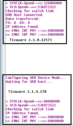
    2. Below g_ui32SysClock  reports 120Mhz for PSYSDIV N3+1,how can the  VCO speed check be correct? Better yet why has Tivaware 2.1.4.178 ignored passed variable (120000000) lowered SYSCLK speed 60MHz? Why is Tivaware 2.1.4.178 SysClkFreqSet() not keeping consistent to earlier Tivaware 2.1.0.12573 SysClkFreqSet() relative to PSYSDIV (N+1) and past in SYSCLK speed 120000000? Could it be ADC0 FIFO speed of SYSCLK being 120MHz was to fast and 60MHz SYSCLK thus fixes some ADC issues? 

    We forced ADCCLK divisor believing forum discussion PLL/2 being default but ADCLK actually ran 60MHz causing analog acquisition problems for periodic signals crossing each 1/4 VREP-VREFN.  

    /* MPU uses MOSC driven PLL 480MHz/4 produce 120 MHz SYSCLK:
       Y1 = 25mHz XTAL HIGHFREQ. */
    g_ui32SysClock = MAP_SysCtlClockFreqSet((SYSCTL_XTAL_25MHZ |
    	                                          SYSCTL_OSC_MAIN |
    	                                           SYSCTL_USE_PLL |
    	                                            SYSCTL_CFG_VCO_480), 120000000);

  • BP101,

    BP101 said:
    You really believe 800mv is the analog resolution

    No, both Ralph and I are saying it is 0.8mV (800uV).

    BP101 said:
    1. PLL seems to be overclocking according to the call back from SysCtlVCOGet().

    You were using the function incorrectly. Please see my previous post and suggested correction to your code.

    BP101 said:
    why has Tivaware 2.1.4.178 ignored passed variable (120000000) lowered SYSCLK speed 60MHz?

    That is not what is happening.  System clock is 120MHz, but VCO is 240MHz.

  • Perhaps that is why 1/2 LSB resolution is called charge sharing of Rs impedance , e.g.  Cext into CADC is an RC charge exchange that does not cause an direct effect upon 3v3 VREF. Charge exchange as defined should help to isolate MCU +2v LDO from the ANIx analog signals. There should be no direct impact on the internal MCU voltages from the analog MUX side of ANIx inputs. CADC is supposed to be the intermediate referee in all charge sharing.

  • Bob Crosby said:
    No, both Ralph and I are saying it is 0.8mV (800uV).

    800uV is far cry better than 800mV, my mistake. According to fig 15-9 1/4 resolution ends at 800mV/4096=201uV 1/4 scale low end resolution. So I don't know where you are coming up with 800uV for 1/4 scale analog resolution. Like I said 800mV though 800uV no better would be the grand canyon of non acquisition not being accepted for most any DSP applications requiring closed loop feed back.

    mV per ADC code = (VREFP - VREFN) / 4096 and the per ADC code infers each 1/4 step in the table gets divided by 4096 produces 201uV resolution, not 800uV. You can't make a formula and later not abide by the math in the formula as it relates to the all ADC codes (levels) in the table.

    Bob Crosby said:
    That is not what is happening.  System clock is 120MHz, but VCO is 240MHz

    PSYSDIV in RSGCLKCTL=0x3 which coincides with SYSCLK speed 120MHz reported in screen shot above not 60Mhz as Tivaware  2.1.4.178, better check again it is producing 60MHz SYSCLK.

    Bob Crosby said:
    You were using the function incorrectly. Please see my previous post and suggested correction to your code.

    The call back SysCtlVCOGet() is a pointer so &'ing the results may not produce correct return if the function is interrupted by NVIC. Will give it a try your way, yet the pointer into an array seems proper way to handle the call back of ( *pui32VCOFrequency = ui32TempVCO;). Still does not answer why SYSCLK was being set 60MHz via Tivaware 2.1.4.178 that was pointed out in above screen shot.

    There is no way the SYSCLK can be 120 60MHz if PSYSDIV was set 0x3 RSGCLKCTL. The ADC misses peak acquisitions of periodic signals when ADCCLK seems to be divided to 60MHz. At least now we are getting peak current detection again 32Mhz ADCCLK.

  • I am not sure what you mean by 1/4 scale resolution. VREFP must be at least 2.4V. VREFN is GND.  So the "resolution" could be as small as 2.4V/4096 or 580uV. What value of VREFA+ are you using?

  • I am not sure how your code is setting up the PLL, but I have attached a project that uses TivaWare 2.1.4.178. It sets the system clock to 120MHz, the VCO output to 240MHz and PSYSDIV = 1 (divide by 2).

     /cfs-file/__key/communityserver-discussions-components-files/908/EK_2D00_PLL_2D00_Startup.zip

  • Bob Crosby said:
    I am not sure what you mean by 1/4 scale resolution

    I was referring to how Fig.15-9 divides any of the 4 quarters into much smaller analog microvolt acquisition points. It's seems you may believe a 1:1 ratio exists between analog and digital scales?

    Point is there are at least 4096 points of acquisition in the first quarter as the formula above it shows, the smallest charge share detection 201uV, 1/4 VREFP-VREFN/4096 or 825mV 1/4 full scale, 201uV 1/4 LSB settling. Settling to 1/2 LSB by definition has to do with the microvolt charge sharing steps of Cext with CADC settling to 1/2 LSB (402uV) or better, 1/4 LSB (201uV). That seems to indicate the smallest settling step 201 microvolts and not the way 3v3 full scale is being divided into quarters in Fig15-9. Judging by the FIFO output below (red box) there appears to be sudden jumps in each 1/4 VREFP-VREFN for no good reason. Would not Fig15-9 produce an analog to digital or 1000:1 ratio in the SAR sample to signal frequency? Another point is cross talk being viewed as 100's of microvolt steps ridding on the charge sharing step of signal and coming from an opposing channel. Even if ADC was 825uV 1/4 LSB settling, it would not be a problem since the smallest step we expect to sample @1mA occurs at 1mV output or 10mV/A in the scope Widget.

    Jump in signal (red box) occurs ADCCLK 32Mhz or 60MHz. ADCCLK (32MHz)  PLL (480MHz) is now acquisitioning the INA signals higher microvolt peaks in the 1/4 settled acquisitions rather than the center regions of each pulse being serialized into FIFO data. Yet the monotonic sampling is a one way ticket up with no down capability reflecting even the FIFO being drained after each sequencer step change. Notice the green boxes have bidirectional ratio metric capability being added from multiples with PWM duty cycles. That some how produce missing linear rise of sample acquisition missing in the (red box). So sampling periodic acquisition points sort of works but not like it should in both directions without adding synchronization of PWM module.  

    Notice below PLL is 480Mhz, SYSCLK 120MHz older Tivaware. Newer version set our SYSCLK 60Mhz yet VCO was still 480MHz / 538Mhz. Something is still not right in ADC clocking, divisor was pushing ADCCLK up to 60MHz making it sample the entire signal with absolutely no ratio metric for the INA periodic signal. The red box is ADCCLK 32Mhz but very choppy and not to scale 4096/480 shown below. The other green boxes have PWM module helping to form a proper reading for the scope Widget and digital readouts. 

  • Bob Crosby said:
    the VCO output to 240MHz and PSYSDIV = 1 (divide by 2).

    Why does new version set VCO=240MHz when 480Mhz was being produced with PSYSDIV 0x3N+1 using the new version Tivaware on our MCU's? Our assumption VCO being 240MHz was making the ADCCLK 60MHz since VCO was truly 480Mhz. The VCO is being forced to 240Mhz by PSYSDIV (0x1N+1) in your CCS debug, but actually VCO was running 480Mhz with PSYSDIV N3+1 on all our PCB's but some how only divided SYSCLK after patching old version Tivaware with newer SysClkFreqSet(). Not so easy to just blow everything away in a project just to update driver library and have hundreds of symbol missing errors eat your day away. The reference of driver library to an existing project imported into CCS project tree and referenced via library include paths does not work as original project root remains with old driver library being searched first before includes of newer libraries. That is sort of a gotcha having to destroy perceived working code by adding more issues of missing driver paths and symbols the new driver library then requires not being found in the root.  

    That said I only patched the new version SysClkFreqSet() into the old version library (cleaned/compiled) and called function by a new name. Obviously something more is at hand if the newest Tivaware code sets PSYSDIV 0x1N+1 or (2). I didn't make the Tivaware patch until labor day so the past VCO always relative to 480Mhz PLL/VCO and not 240Mhz. The new version Tivaware may have a MACRO or register calls miss-behaving!

    Perhaps there is an issue with a certain lot of MUC's from production which cause an issue of PSYSDIV not setting correct VCO?

  • BTW the INA output analog signal is somehow being inverted from the FIFO read data or low pass filters. It is upside down when compared to the original INA output analog signal of all scope captures.
  • BP101 said:
    I was referring to how Fig.15-9 divides any of the 4 quarters into much smaller analog microvolt acquisition points.

    I think you are misinterpreting figure 15-9.

    This figure shows that the result of the conversion for 1/4 (VREFP-VREFN) to be 0x400, or 1024. At 1/2, the result is 0x800 or 2048. At full scale, the result of the conversion is 0xFFF or 4095. With VREFP = 3.3V and VREFN = GND, 3.3V/4096 = 0.000806V, 0.806mV or 806uV. This is the size of one LSB (least significant bit).

  • Hi Bob,

    Bob Crosby said:
    am not sure how your code is setting up the PLL, but I have attached a project that uses Tivaware 2.1.4.178. It sets the system clock to 120MHz, the VCO output to 240MHz and PSYSDIV = 1 (divide by 2).

    Yet your screen shot shows PLL 480MHz and PSYSDIV=1N+1 (div/2) should make SYSCLK=240MHz, not 120MHz reported. This seems to be where wires are being crossed between older Tivaware & newer versions. The older version SysClkFreqSet() 480MHz PLL with PSYSDIV (2N+1) divide by 4 also reports SYSCLK being 120MHz. How can that be if the newer version has the same 480MHz PLL called with the same passed in variables? Basically what Tivaware 2.1.4.178 is indicating PSYSDIV register has no ability to divide 480MHz PLL by 4? Yet SysCtlVCOGet reports 480MHz in both versions of SysClkFreqSet() when 2.1.4.178 was patched into 2.1.0.12573 with unique name being called in the application. The only difference is SYSCLK was 60MHz (2.1.0.1273) indicating it actually pre-divides SYSCLK without the use of PSYSDIV register control. Otherwise SysCtlVCOGet() returns the same 480MHz VCO speed for both versions and can not be fully trusted. This indicates TI programmers did not do regression testing on older versions and expect the community to bend without full explanation being presented in Wiki report format!

    It seems your SYSCLK speed value above is being forced 120MHz (2.1.4.178) in your screen shot. The net result is the ADC0 FIFO runs at a much higher speed (240MHz?) to keep pace with the much faster ADCCLK (60MHz) and not 32MHz as the datasheet is telling us it must be for 2MSPS. How can we buy the fact PLL is dividing 240MHz without PSYDIV according to main clock tree Fig 5.5 being consistent in that very detail? If the main clock tree is not drawn correctly perhaps an updated Fig 5-5 would behoove the community?

    That is perhaps why the acquisition points in the analog signal change with much faster FIFO keeping more synchronous with converter, yet to test this. The problem was my SYSCLK speed to the FIFO was still 120MHz. My patch of 2.1.4.178 SysClkFreqSet() into older Tivaware again reports SYSCLK=60MHz with PSYSDIV 3N+1 (div 4), verified CCS debug. According to clock tree Fig. 5-5 (2.1.4.178) somehow pre-divides SYSCLK, perhaps Fig. 5-5 drawn incorrectly? Perhaps the ADC block receives VCO (480MHz) into FIFO prior to slower ADCCLK divisor of AD converter? That would be more believable in the context of PSYSDIV, VCO and Fig.5-5 which this post seeks to clarify exact details, not simple suppositions or WA's without being very clear of the intent relative to Fig 5-5. One belief is R2 silicon is not an errata imposed on PSYSDIV control register that was not discovered during R1 production testing and to the degree 2.1.4.178 has tired to force a WA. 

    Scope widget (older SysClkFreqSet()) shows sampled peaks of analog signal being excessively high, (ADCCLK/8=60MHz, 480MHz PLL). SYSCLK reports 120MHz, PSYSDIV=3N+1 divide PLL/4. Also notice the scope widget signal is not inverted but never could properly settle to 1/4 LSB or even to 1/2 LSB peaks and caused over current trip faults, shutting the system down. The INA periodic input source 3 AINx channels can perhaps verify the ADC0 FIFO clocking is keeping to datasheet INL +/-3LSB specification. We never could reach the true current measure with ADCCLK/8 (60MHz) indicated in Widget actual average current  7.9-8.4 amps being completely missed. How could the datasheet be so wrong and production silicon testing miss 2MSPS requires 240MHz PLL? The widget may be telling the truth in the matter of Who's on first.

  • Bob Crosby said:
    At full scale, the result of the conversion is 0xFFF or 4095. With VREFP = 3.3V and VREFN = GND, 3.3V/4096 = 0.000806V, 0.806mV or 806uV. This is the size of one LSB (least significant bit).

    I don't believe that is the case, here's why.

    Settling to 1/2 or even 1/4 LSB occurs relative to full scale -VREFP (3v3) or 4096 in each of the (digital) millivolt quarters.

    So I disagree 806uV being smallest acquisition since you did not divided each 1/4 by the full scale digital value -3v3 VREP. The equation (mV per ADC code) indicates we divided each 1/4 ADC code by 4096 for the ADC codes shown left side of graph, not just the full scale being divided 4096. What do you think the ADC codes are if it not the values on the left side of the graph? Should we disregard the equation being presented also clearly stating (per ADC codes) left side of graph.

    If they did not intend division by full scale  VREFP (4096) to determine each 1/4's smallest LSB the graph should not be divided into 1/4 ADC codes referenced in the equation. Otherwise table graph ADC codes (left side) have no reference point to bottom scale other than +VREFP (3v3) and that is not the definition of 1/2 LSB being settled for CADC in any 1/4 of ADC codes.

    My equation for each 1/4 LSB settled acquisition: 0.25*3.3=0.825/4096=0.000201V or 201uV.

  • BP101,
    I agree that 1/4 LSB is 201uV, but the ADC resolution is 1 LSB (806uV), not 1/4 LSB. The application note that suggest using an external capacitor that gives a settling time to within 1/4 LSB during the sample window, does not imply a 1/4 LSB resolution on the ADC. Any mismatch of the external voltage to that of the sample capacitor will add to the total error.

    Assume a perfect 12 bit SAR ADC with 3.3V reference. Provide a 807uV input. The perfect ADC will resolve the output as 0x001 because 807uV is greater than 806uV but less than 1612uV. To the perfect 12 bit 3.3V ADC, all inputs between 806uV and 1611uV are converted to 0x001. There is no way for this ADC to distinguish or uniquely represent those two voltages. There is no hidden scaling.

    Any results taken with ADC clock at 60MHz are invalid and should be ignored.
  • BP101 said:
    Yet your screen shot shows PLL 480MHz and PSYSDIV=1N+1 (div/2) should make SYSCLK=240MHz, not 120MHz reported.

    No, what my screen shows is that if I call the function SysCtlClockFreqSet requesting 480MHz VCO using TivaWare v2.1.4.178 it sets the VCO to 240MHz.

    	g_ui32SysClock = SysCtlClockFreqSet((SYSCTL_XTAL_25MHZ |
                                           SYSCTL_OSC_MAIN |
                                           SYSCTL_USE_PLL |
                                           SYSCTL_CFG_VCO_480), 120000000);
    

    The function still set the PSYSDIV so that the system clock is 120MHz as I requested. The only issue is how to setup the ADC clock. This was done because of erratum SYSCTL#22. Sometimes (rarely) the PSYSDIV does not properly load to the actual divide circuit. So instead of getting the divide ratio you want you get divide by 2. When the VCO is at 480MHz, it tries to run the part at 240MHz and the part hangs up. To avoid this issue, TivaWare version 2.1.3 and later modified  the SysCtlClockFreqSet function to not use 480MHz.

  • Bob Crosby said:
    I agree that 1/4 LSB is 201uV,    but the ADC resolution is 1 LSB (806uV), not 1/4 LSB.

    100% AGREE (even 'LIKE') and as (another) 'outsider' - I've 'NO Dogs in this Fight!'    Thus 'Zero' pre-bias.

    Having employed ADCs (long) before they (ever) appeared w/in MCUs (my past firm often purchased (Premium) ADCs from 'Burr-Brown' (past acquired by this vendor) I believe (somewhat) 'informs & advises' my agreement w/Vendor's Bob - indeed there is   NO/ZERO 1/4 LSB resolution!

    Such proves a CLEAR MISUNDERSTANDING (No matter how often protested/repeated) on poster's (sole) part!     (Has not a tendency to 'reach' (come to improper ('hoped for' conclusions) been past noted?)

    This argument (NO 1/4 LSB resolution capability) can be STRENGTHENED  via simple analysis of the Business Side - as well as the Tech Side.  (Bob's side)     

    Would ANY MCU Vendor - when offering a 'FOURTEEN BIT ADC'  (which results should '1/4 LSB' prove valid)  ...  withhold   that (competitively HUGE) information?     Or - promote that 'Key Advantage' - ONLY  w/in some (effectively unknown) arcane App Note?     Of course not!     (and  HOW - has that been MISSED?)

    Rather than 'Bend the real-world' to an 'Incorrect Conclusion' (no matter how 'hoped') - the 'Acceptance of Reality' - proves FAR Superior...

  • Bob Crosby said:
    . When the VCO is at 480MHz, it tries to run the part at 240MHz and the part hangs up. To avoid this issue, TivaWare version 2.1.3 and later modified  the SysCtlClockFreqSet function to not use 480MHz.

    That obviously confuses the discussion for anyone not loading driverlib 2.1.3 or above besides making the ADC clock divisors a more confusing point in forum discussions, as it did. So the ADC is behaving very strange with 480MHz PLL ADCCLK div 8 seemed to produce 60MHz or 4MSPS, made the FIFO scope data appear non-inverted. It did not seem to heat the MCU or cause any other issues other than settling acquisition being left at the curb.

    BTW: The TM4C1294 ADC is a precision SAR and I would expect far better than 800uV resolution as that infers better than near 1mV resolution. Certainly 201uV resolution would be worthy of the SAR being (precision) in 1/4 LSB settled acquisitions. I don't think it proper to say near 1mV resolution is anywhere close to being a precision SAR even with +/-30 LSB error in the mix.


  • Bob Crosby said:
    I agree that 1/4 LSB is 201uV, but the ADC resolution is 1 LSB (806uV), not 1/4 LSB.

    I don't think that is what the application text is suggesting about 1/4 LSB but the 1 LSB resolution is 201uV the smallest value of acquisition Fig 15-9 or it would not be a precision SAR rather a very imprecise SAR at best. So near 1mV resolution in todays world is dirt poor, my cheep 6000 count DMM has better uV resolution, thus find it hard to believe 806uV with +/- 30 LSB seemingly would make an even worse than poor resolution.

    Text below is generic for 12 bit 16 channel SAR with 20pf CADC, it pretty much covers the more advanced 20 channel SAR capability since it predates the newer silicon in the TM4C129x MCU class. Don't you agree precision should not be any less than previous Stellaris M3 class SAR being replaced by newer M4 class SAR devices with more favorable advances, should improve precision in that update process?   

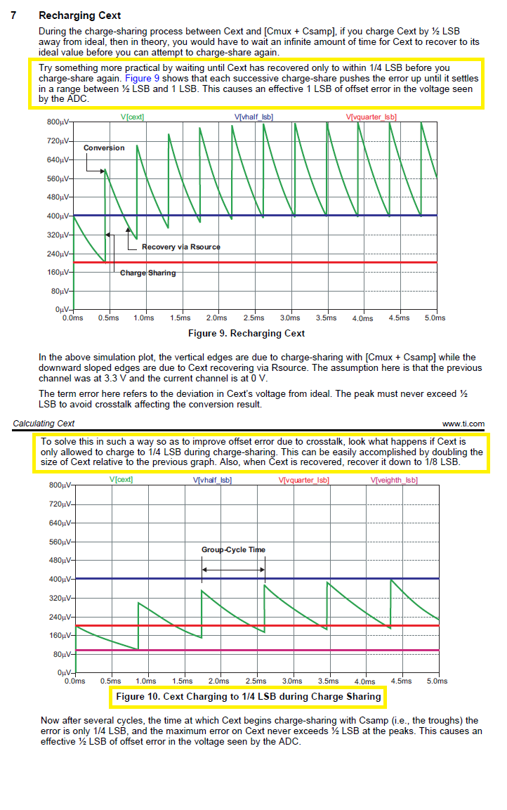
  • So the INA240 output peeks were much wild like Fig 9 with Cext (1n, 10n, 15n) and seemed to exceed 1/2 LSB error. Doubling Cext (22n) stretched out and lowered peak 1/2 LSB error over 80us period hopefully keeping error to 1/4 LSB. Channel sample timing around Cext sharing attempts to keep the window tight around the cycle group peak time and not saturate the ends (VREFN, VREFP) so much with lower signal noise.

    That terminology (LSB) seems to infer 1/4 LSB down to 0V being bits, not a single bit. Though is not 1/4 LSB (Fig. 10) starting near 200uV in the simulation of PSpice for Cext value. I wonder why the TM4C1294 would not have 20uV analog resolution since the 80uV was several years prior technology including several different SAR's.
  • BP101 said:
    I wonder why the TM4C1294 would not have 20uV analog resolution

    We'll have to 'break-out' our 6th grade 'math book' - to resolve this one.

    Assume the same 3V3 (or 3300mV  or  3,300,000µV) as ADC's 'Full Scale Voltage.'

    Then ...  3,300,000µV / 20µV  =  165,000.    This (165K) represents the 'resolution' enforced upon such an ADC.

    We 'know' that 12 bits yields 4,096 unique ADC counts or values - 16 bits = 65,536 (unique counts or values) thus 'An EIGHTEEN BIT ADC would be REQUIRED - to meet  your (latest) DEMAND!

    Stand clear of any/all vendor pathways - as they RUSH - to MEET your latest demand...      Your  'reading up' -  on the limitations which 'Mixed Signal' devices - impose upon  Analog capability - may (reduce) your 'wonder.'

  • cb1_mobile said:
    We 'know' that 12 bits yields 4,096 unique ADC counts or values - 16 bits = 65,536 (unique counts or values) thus 'An EIGHTEEN BIT ADC would be REQUIRED - to meet  your (latest) DEMAND

    I was referring to the analog side of the equation, not a digital calibrated SW equivalent. So 20uV resolution in 3v3 full scale would be settling acquisition, that has nothing to do with the digital results in 3v3 full scale

    Settling is typically 1000:1 ratio (analog to digital conversion) in older M3 SAR, stands to reason 5k:1 would be the next M4 evolution in SAR accuracy by design. Like wise LSB 0V (0x000) and figuring 1LSB (0x001) could only be an equivalent analog measure to near 1mV (805uV) seems a huge misnomer in the definition of settled analog acquisitions.

    Actually 0x001 can be anything you want it to represent digitally, from the analog acquisition perspective as long as the ceiling is know in 3v3 full scale. Trying to squish 12bits (0-4096) into 3v3 to achieve a 1:1 AD ratio when the ratio is 1000 or more to 1 seems wrong. Effectively the smallest settling acquisition point becomes the floor 0x000, the ceiling 0xFFF of all acquisitions. We can make the floor be 1uV, that does not mean the SAR can sample analog that low but it sure as heck can sample a lot lower than 805uV. I'm even thinking 201uV is way off from the reality of 0LSB up to 1LSB. That indeed is the missing puzzle piece being left out of all electrical specifications or conversion topic and replaced with SNR and 20 oversamples required with internal reference to achieve +/-3LSB gain error. Yet the M3 SAR datasheet show +/-3LSB with internal reference and the newer M4 +/-30LSB any single sample is beyond belief TI would go backwards.

    Again cheep DMM can measure 750mohm shunt down to 1uA but the TM4C SAR chokes to follow INA signal. Yet the DMM measures same current point with no issues without having PWM module to assist it. That alone indicates there are more problems with TM4C1294 SAR than has been admitted in this forum setting and laboratory analysis would reveal what why and how of it all. 

    q. Et +/-30 LSB = Total Unadjusted Error is the maximum error at any one code versus the ideal ADC curve. It includes all other errors (offset error, gain error and INL) at any given ADC code.

    Why does the M4 leave Et unadjusted when the M3 shows +/-3 LSB for the same internal reference? Does this not appear as a step backwards or were the M3 SAR results being fluffed?

  • What I see going wrong with the TM4C SAR, digital converter fails to subtract VREFP (3v3) from the converted results placed into FIFO after hardware averaging.

    Perhaps why the scope widget above (red box) dose not flow smoothly relative to sampled acquisitions of the INA240 rising periodic signal. The PWM duty cycle fixes the converters ratio metric error 2MSPS (Tc = 4 ADCCLKS @32MHz) not 16 which may further exacerbate the issue. As I recall even the M3 failed to properly digitize the INA282 output signal in proper ratio metrics, same issue has existed across several silicon designs. The M3 was multiplying the sample amplifier bias time 3 million and arriving at ratio metric result the SAR should have been providing from settling to 1/4 LSB -3v3 VREFP.

  • BP101 said:
    I was referring to the analog side of the equation, not a digital calibrated SW equivalent. So 20uV resolution in 3v3 full scale would be settling acquisition, that has nothing to do with the digital results in 3v3 full scale

    Let us - for a moment - 'accept' your view (above.)      What then is the (possible) value of such 20µV resolution - as it  CANNOT be PRESENTED to the ADC User?

    Again - returning to REALITY - your belief in (either) 20 or 200µV resolution - from a 'low-cost' Mixed Signal Device - proves once more  (so very) FAR from REALITY!

  • I just want to clarify a few things for the few brave people who have followed this thread to this point.

    The total error for the TM4C129 ADC is +/- 30 LSB when it is clocked at 32MHz. (2Msps). The total error is +/-4 LSB when clocked at 16MHz. It is better to do a single conversion at 16MHz ADC clock than to do a 2 sample hardware average with a 32MHz ADC clock. They both take the same amount of time and produce a net sample rate of 1Msps, but the slower ADC clock rate will give more accurate results.

    BP101,

    As I tried to explain before, the recommendation that you use an external capacitor such that the sample capacitor can settle to 1/4 LSB in the sample time does not imply that the precision of the ADC is 1/4 LSB. If you do not believe me, let's just agree to disagree. If the 805uV precision of the TM4C1294 device is not adequate for your application, I suggest you look elsewhere.

  • Bob Crosby said:
    The total error for the TM4C129 ADC is +/- 30 LSB when it is clocked at 32MHz. (2Msps). The total error is +/-4 LSB when clocked at 16MHz. It is better to do a single conversion at 16MHz ADC clock than to do a 2 sample hardware average with a 32MHz ADC clock. They both take the same amount of time and produce a net sample rate of 1Msps, but the slower ADC clock rate will give more accurate results.

    May a (very) loud 'BRAVO' - echo across this dead/dying thread.    (at least that is hoped)

    Note that vendor's Bob provided a 'Crisp, Clear Tech Description' - devoid of (any)  'opinion'  - and came to a 'Highly Effective' (and poster-specific) recommendation - extremely tied to 'KNOWN FACT!'    

    And - even better - that 'use of a 16MHz ADC Clock - offers up a substantial, 'increase in ADC accuracy' - for SO MANY here!     (again - as Bob noted - for those (very) few - remaining...)

  • Hi Bob,

    Bob Crosby said:
    If the 805uV precision of the TM4C1294 device is not adequate for your application, I suggest you look elsewhere

    It's not that I don't believe what you are saying, rather that it doesn't relate to the issue of ratio metric failure being reported across several posts, both M3 and M4 SAR ADC. Even 805uV precision should not be a problem for 10mV/Amp scale. Yet the SAR can not properly function @10mV let alone 201uV or even 805uV, both are mute points.  

    When the ratio metric SAR can not properly resolve a rising periodic signal at any sample rate (1 or 2MSPS) there is something seriously wrong. I still suspected FIFO clocking as the 60Mhz ADCCLK produced non inverted near (real time) acquisition without lagging behind the application interrupt handler. We can live with precision errors yet issue goes beyond that. Seemingly SAR is unable to resolve ratio metric (periodic) analog slope in a signal via converters handling VREFP-VREFN relative to any 1/4 ADC codes Fig. 15-9. The INA240 was designed proven to work with SAR ADC, per technical disclosures in the analog cook book and other marketing documents.

    The INA240 analog signal should be easily followed by M4 SAR with ratio metric monotonic sloping, both directions. Yet scope Widget (red box) fails in either direction to properly follow (10mv/Amp) in the open loop gain of INA240 input to single ended AINx channel. The jumps you see in the scope widget (red box) are seemingly the converter/averaging not updating the FIFO in real time and it lags behind interrupt processing of the sample. Ratio metric slope production fails 1 or 2MSPS with or without hardware averaging, logical deduction it simply don't work. 

    The ADC0 sequencer 1 is priority 2 and has higher NVIC interrupt (INT31) and lower priority (0x40) than PWM0 (INT26/27) priority (0x20). Is it possible NVIC priority of FIFO and circular reads during interrupt handling has something to do with INA missing slope data?  If you truly believe the M4 SAR should produce ratio metric slope @10mV/Amp acquisition points from the INA240 output signal why does it fail to do so? 

        /* Configure GPIOADCCTL REG23 0x530:
         * Trigger ADC0 SS1 samples via GPTM oneshot 1.5us blanking timer
         * fired at each commutation of PWM0 output control block
         * Assign the ADCEMUX  2nd highest priority to ADC0 SS1. */
        MAP_ADCSequenceConfigure(ADC0_BASE, 1, ADC_TRIGGER_TIMER, 1);
    
        /* Hardware oversampling is enabled at 2MSPS.
         * NSH16/1.143Msps: 2xOVS=571.5KSps
         * NSH8/1.6Msps: 2x OVS=800Ksps
         * 0x0=NoAVG, 0x1=2, 0x2=4, 0x3=8, 0x4=16, 0x5=32, 0x6=64 */
         HWREG(ADC0_BASE + ADC_O_SAC) = 0x1;
    
            /* Increase step sample hold time for this sample sequencer.
             * @32Mhz:Nsh(4) =Tshn0x0 encoding, Rs250  Ohms 2.0Msps
             * @32Mhz:Nsh(8) =Tshn0x2 encoding, Rs500  Ohms 1.6Msps
             * @32Mhz:Nsh(16)=Tshn0x4 encoding, Rs3.5k Ohms 1.143Msps
             * @32Mhz:Nsh(32)=Tshn0x6 encoding, Rs9.5k Max, 727Ksps */
            HWREG(ADC0_BASE + ADC_O_SSTSH1) = 0x2222;
    
            MAP_ADCSequenceStepConfigure(ADC0_BASE, 1, 0, PIN_IPHASEA);
            MAP_ADCSequenceStepConfigure(ADC0_BASE, 1, 1, PIN_IPHASEB);
            MAP_ADCSequenceStepConfigure(ADC0_BASE, 1, 2, PIN_IPHASEC);
            MAP_ADCSequenceStepConfigure(ADC0_BASE, 1, 3, ADC_CTL_END | ADC_CTL_IE);


  • BP101,
    I am afraid that all of the discussion on precision has been a rabbit trail that has not been of benefit to either of us. A discussion on the FIFO clocking scheme will be equally unhelpful. Would you please help me isolate your problem by some experiments.

    1. Yes, the TM4C1294 ADC is 1:1 in that when using a 3.3V reference, 3.3V in gives 0xFFF as a result. 1.65V in gives 0x800. Do you suspect that you are getting values "scaled" instead? If so, please input a DC voltage to the ADC and check the results. If they are 1:1, we can move to the next step. If not, we must resolve that problem before continuing.

    2. Are you getting the sample rate you expect. First, analyzing the code you posted above, I calculate your sample rate as: 200K samples/second, or sampling each phase every 5uS. This assumes that you only use sequence 1. That calculation came from 32MHz ADC clock divided by 20 clocks per sample (8 sample and hold + 12 conversion) gives 1.6M samples/s. Using 2x hardware averaging cuts the effective sample rate in half, 800K samples/s. You are sampling 4 channels, which means each channel is sampled at 200K samples/s, or once every 5uS. As I mentioned earlier, I suggest you go to a 16MHz ADC clock and not do the 2x hardware average. Also the output impedance of the 1NA240 is low enough you should not need the extra sample time. Making those changes would increase your sample rate to 250K samples/s and improve the accuracy. To verify that the sample rate is correct, I suggest you use a function generator and apply a 3V sine wave (0 to 3V) at 20KHz to one of the inputs. You should then see the sinusoidal pattern repeat every 10 samples. If not, we need to resolve that problem before continuing.
  • Bob Crosby said:
    The total error is +/-4 LSB when clocked at 16MHz. It is better to do a single conversion at 16MHz ADC clock than to do a 2 sample hardware average with a 32MHz ADC clock. They both take the same amount of time and produce a net sample rate of 1Msps, but the slower ADC clock rate will give more accurate results.

    The difference is the 2MSPS doubles the acquisition points in the analog signal being sampled increasing precision further by hardware averaging, 1MSPS can not compete with that precision gain. That is the entire concept behind 2MSPS increase the granularity in the analog sampling time frame. Really to strange neither sample rate can read the INA240 (10mv/Amp) open loop gain as it should.

    Oddly EK-TM4C1294XL ADC0 SS1 is scanning INA240 ANIx (open) channels for current samples during application runtime or idle time. DMM voltage slowly drops from 1.2v down to 0.5mV, cycles over again. As the sequencer steps seem to enter acquisition on each open ANIx channel during run time the pins float near 108mV. I think it very odd any thing over few millivolts being present on an ANIx open input when they are designed to limit channel cross talk.

    The INA240 output pulls down each AINx to 1.2mV-1.8mV via 2k series R during idle time. Expect each ANIx pin attempts to float near 108mV during run time too. That seemingly explains why the open loop gain is much higher than expected after increasing the Cext value. 

  • To end this thread I'd like to thank Bob for his very clear instruction of which was applied to the production system with no net gain. So the issue of 1MSPS versus 2MSPS, 1/4 LSB, or disabling hardware averaging did not improve granularity of samples nor produce monotonic ratio metric slope in the scope Widget current trace.

    Fact is the FIFO data LSB is not reducing the steps in (red box) of Widget signal when the FIFO array variable instead required being forced to zero via software. That stair stepping of scope Widget signal was primary clue the AD converters FIFO data looses control of the closed current loop from the configured steps of the sequencer.