This thread has been locked.

If you have a related question, please click the "Ask a related question" button in the top right corner. The newly created question will be automatically linked to this question.

EK-TM4C1294XL: ADC channel differential

Guru 56103 points
Part Number: EK-TM4C1294XL
Other Parts Discussed in Thread: LM94022, INA240

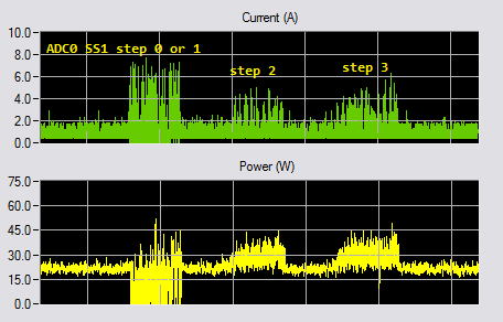
After more KISS testing of ADC0 SS1 step 0 or 1 FIFO1 data seems to produce differential signals in scope widget. However step 2 or 3 if step 0 is disabled, step 1 seems to produce the same results shown below. The digital value reading of step 1 traverses far more negative than the scope widget can show. 

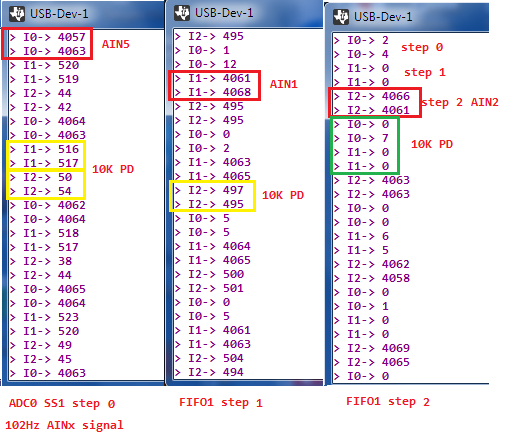
How can input differential mode be set on a channel pair, e.g steps 0 or 1 when it was not configured via software? In the code below the same differential output results for step 0 or 1 if the FIFO is pre triggered to render the results of next step. Does it not appear a differential exists in the same signal be placed on AIN5, AIN2, AIN1? This is driving me crazy since it does not add up to being typical behavior of matched channel Rs impedance. What would cause the AIN channel to allow input signal below the others? It would seem this issues can also lead to unrestrained VREFN saturation.

//MAP_ADCSequenceStepConfigure(ADC0_BASE, 1, 0, PIN_IPHASEA);
  MAP_ADCSequenceStepConfigure(ADC0_BASE, 1, 1, PIN_IPHASEA); // AIN5
  MAP_ADCSequenceStepConfigure(ADC0_BASE, 1, 2, PIN_IPHASEB); // AIN1
  MAP_ADCSequenceStepConfigure(ADC0_BASE, 1, 3, PIN_IPHASEC | ADC_CTL_END | ADC_CTL_IE); // AIN2

  • So you are not in differential mode, correct?

    I'm not sure what you are trying to show here. Can you create an excel table clearly showing what channels are mapped to what sequence steps and what voltage is applied to each channel and what is read from the FIFO for each channel. Start with a fixed voltage such as 0v or 3.3V and if you think there is noise injected between channels then record the RAW FIFO values. For example, if a channel is connected to 3.3V then the expected value is 4095. You have come up with many scenarios where the channel can lose its accuracy. At which exact circumstance did you see the converted result not equal to 4095?
  • Hi Charles,

    Correct SS1 of either ADC module are not being configured for differential AINx inputs. That does not mean differential configuration in not occurring via some other unknown or undetected reason. Results might go unnoticed if differential mode is switching back and forth of any single input source during FIFO shifting of acquisitioned samples. Yet it become clear when non periodic signal are injected direct AIN inputs being VREFN or VREFP, e.g. 0v or 3v3 and nothing in between these two voltages, 1/2 VREFP occurs. 

    There is no reason the first or second configured step of FIFO1 read data should produces scope signal shown in widget for single ended AINx signal source.  Signal happens to be 60Hz, none the less datasheet SNR % is not keeping consistent between channels (scope widget), we must ask our selves why? Scope widget indicated a differential is occurring in AD conversions shifted into  FIFO1, for unknown reasons. Even the LM94002 temperature FIFO1 is retuning 1/2 values of full VREFP for any AINx inputs configured step 0 or 1 as if being merged, 1/2 VREFP is produced in FIFO1 solution again indicating differential AINx behavior. Yet another direct indicator somehow differential mode has been configured for AIN channel inputs step 0 or 1 and NOT specifically configured to do so by Tivaware as indicated in datasheet sequencer register POR reset defaults.

    Sequencer step 0 or 1 somehow become configured in differential channel mode and divide VREFP/2 (1.65v) values for any second step reads of returned FIFO data. That occurs no matter if END is placed after the last step with AINx input source or on the last step without AINx input source.

    This issue seems more sequencer configuration related, how to stop the input channels from defaulting to differential after POR? It may not seem possible for differential FIFO data yet it is occurring in both ADC0 SS1 steps 0/1 and ADC1 SS1 steps 0/1. Yet the differential (1/2 VREFP) seems to stop after the next configured step relative to all configured sequencers steps that are not differential related to AINx channel assignment of the first step. That is what the above scope widget is also indicating and the LM94022 captured results in last post. Both are periodic analog signals in the interrupts of the application handing of the FIFO results data relative to AINx source and AD converters acquisitions  of each static signal. 

    It's no wonder the LM94022 sensors FIFO values can not properly stabilize from any 16:0 AIN inputs as second step FIFO data is randomly 1/2 VREFP. Source code was provided for TI to investigate how it is occurring. This also answers why INA240 monitors on ADC0 SS1 can not produce correct current reading when 1/2 VREFP values are occurring on step 2 of the read FIFO data.  

  • CCS Debug REG 16 ADCSSCTL0 is 0x0 no Dn bits are not set. Does that mean the GEL file is correctly reading the register or CCS debug is showing the actual configuration? For instance the Head and Tail pointers are always equal in value, 100ms register refresh intervals and simply can not be the truth. Status of FIFO underflow overflow only seem to occur during slow debug application Run and don't move in debug register view, only via  UARTprintf() do we know it ever occurs but only underflows during debug.

    Below testing of ADC0 SS1 steps 0-2 with 102Hz GPTM input signal moved to next AIN input in each frame. The odd part is the cleared interrupt seems re-entrant in each step of the FIFO read process.  Odder observation is FIFO overflow seems to occur 102Hz AIN steps (red box) into the next FIFO read step (yellow box). That seemingly is impossible via the application that reads PWMENABLE register bits being AND (IF,ELSE IF, ELSE) on each 3 reads of the circular FIFO each directive tested.   The FIFO Is drained between reads into the C+ array variables after each directive is tested for AND match of PWMENABLE register bits.

    How is the next step/s FIFO value (yellow box/s) changing if not by unreported undetected FIFO overflow? Otherwise Dn bits (step 0-1) ADCSSCTL0 actually being set and not being reported? If result is considered channel isolation specially designed to limit cross talk, smoking mirrors comes to mind. Special notice of last column after step 2 (green box) has no overflow data step 0 or 1, why?

  • Oddly the scope signal shown step 0 in 1st post CH5 may be status underflow related but who could consider that was occurring, datasheet appears to have disclosure voids. The AD converters digital scale Fig15-9 is depicted as producing Unsigned integers only, yet plain as day the scope widget shows negative integers were occurring from an AC signal input on a perceived single ended AINx channel.  

    ADCUSTAT and ADCOSTAT (REG5/7) RWIC do not seem to always assert from C+ cyclic updates via OR Equals (|=) symbolic naming convention. That seems to suggest Fig.15-9 has not told the entire truth of VREFP-VREFN.

    As for the unreported FIFO overflow condition shown above capture (ADCOSTAT) RWIC bit check is not reporting an overflow occurred/s. Perhaps even during FIFO draining after an underflow somehow causes FIFO overflow of unsigned integers being dumped into the next step! That might have been a datasheet fact being omitted not only in earlier M3 class ADC but also the later M4 class ADC modules. 

    There is an answer for behavior and Tivaware also has not come close to properly handling FIFO data for business related purposes of M4 class ADC module. TI forum employees suggesting ACDSecquenceDataGet() being superior or the only supported method for reading FIFO data is leading the TM4C1294 community into a black hole of singularity! This thread is how KISS works in the real world, make it work right! 

  • Locking down ADC1 SS1 tail pointer to specific steps during interrupt handling disrupts ADC0 SS1 step 0 making it differential. Step 1 & 2 of ADC0 SS1 then cascade values.

    FIFO1 seems to divide acquisitions between the steps of ADC0 and ADC1. The FIFO tail pointer looses BASE perspective of which ADC module FIFO1 belongs/ed too when the END IE occurs. If ADC1 SS1 tail pointers are not locked as shown below then the ADC0 SS1 has the behavior shown in capture above.

    Odd ADC module behavior with SS1 is not listed in data sheet nor errata document. So it not fair to say Tivaware ADCSequenceDataGet() works any better than HWREG macro FIFO reads. Software checking ADCSSFSTATn register tail pointer values is the proper way to insure the FIFO step results are aligned with the intended data of the ADC modules BASE address 0x4003.8000 or 0x4003.9000 of the specific sequencer and step that stored the data. It would seem unconstrained SS1 meanders between ADC0 and ADC1 modules at the wrong timing. That is why it is so difficult to pin SS1 down when both ADC0 and ADC1 share the FIFO1 between them but incorrectly.

    ADC1 SS1 constrained ADCSSFSTAT code in interrupt handler: 
         
    /* Read sensitive RAW sample sequence steps ADC1 FIFO-1. */
    if(HWREG((ADC1_BASE + ADC_SSFSTAT1_TPTR_M) == 0x0))
    {
      int16ADC1MOSTempLow[0] = HWREGI(ADC1_BASE + ADC_O_SSFIFO1) & 0x0FFF; 
    }
    
    if(HWREG((ADC1_BASE + ADC_SSFSTAT1_TPTR_M) == 0x1))
    {
      int16ADC1MOSTempHigh[0] = HWREGI(ADC1_BASE + ADC_O_SSFIFO1) & 0x0FFF;
    }
    
    Constraining tail pointer ADC0 SS1 the FIFO data becomes differential.
          
            // If GEN1 Low side of Phase A is active, enable
            // current readings on Phase A analog signal.
            if(((ui16PWMEnable & 0x8) == 0x8) &&  
                    (HWREG(ADC0_BASE + ADC_SSFSTAT1_TPTR_M) == 0x0))
            {
                // PIN_IPHASEA Channel 5 ADC0 SS1 step 0
               /* Phase current index */
                g_ucCurrentIndex = 0;
    
               // Read the next sample for the current calculation.       
                ui16PhaseRaw[0] = HWREGH(ADC0_BASE + ADC_O_SSFIFO1);
    
               //USBprintf("> I0-> %i\n", ui16PhaseRaw[0]);
               //GPIOPinWrite(GPIO_PORTB_BASE, GPIO_PIN_3, 0x00);
            }
    

  • It is impossible to constrain both ADC0 with ADC1 FIFO1 via ADCSSFSTAT TPTR bits in the above code and retrieve any data from the ACD0 SS1 FIFO steps at the same time. It seems anyone using ADC1 SS1 and ADC0 SS1 with overlapping steps and different AINx are not getting the results that should be returned from the actual sequencer steps that were used to sample the analog signal, only in one ADC module not both.

    Hardware is flip flopping sequencer step results of the ADC modules shared FIFO1 out of sync with the application checks of ADCSSFSTAT TPTR bits!