This thread has been locked.

If you have a related question, please click the "Ask a related question" button in the top right corner. The newly created question will be automatically linked to this question.

TM4C1294NCPDT: Issues in accessing through I2C registers with two bytes address

Part Number: TM4C1294NCPDT
Other Parts Discussed in Thread: LMK05318,

I am making some tests in order to write and read, using TM4C1294 microcontroller and I2C protocol, LMK05318 registers. 

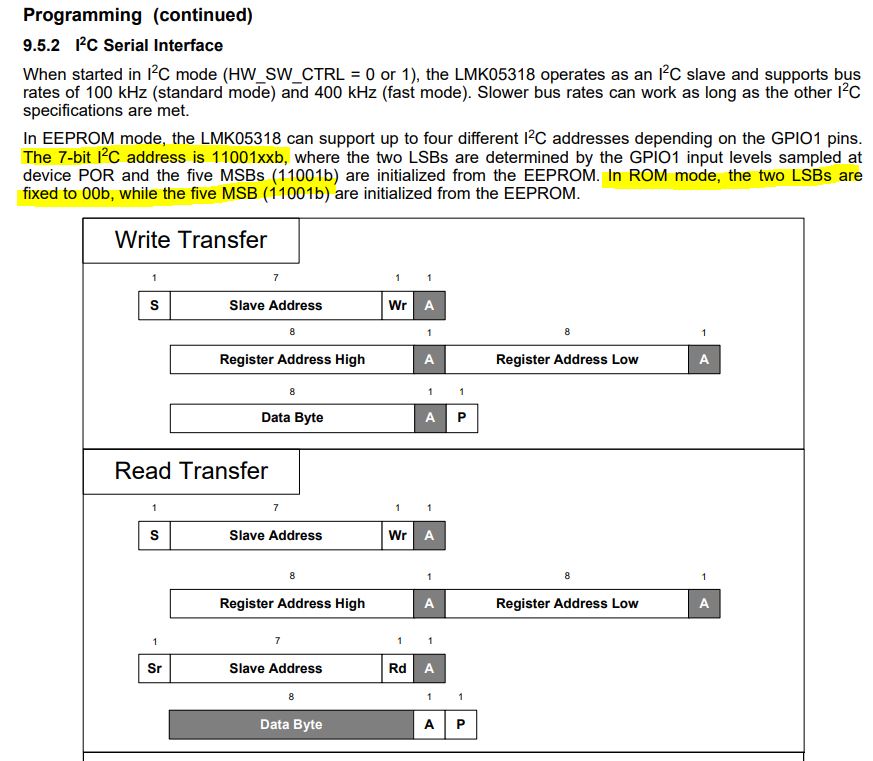
LMK05318 has registers made-up of two bytes (however, only the nine less significant bits are used ). Instead, the length of each register's content is 8 bits.

I2C is working in fast mode

The issue is that  only one of the register's address bytes is sent through I2C.

If I write the register with the address 0x013F (the register's content is 0x18), the logic analyzer shows that the second byte 0x3F is not sent. Therefore, only the following bytes are sent through I2C: 0xF0 (device address) 0x01,0x18.

Instead, when the register is written with "TicsPro" software, the logic analyzer shows that all the bytes are transmitted: 0xF0, 0x01,0x3F, 0x18 (0xF0 is always the device address)

I have also made a test by  inserting the expression I2CMasterBurstLengthSet (I2C5_BASE,3) before the transfer of the three bytes begins. With this expression, the logic analyzer shows that the following bytes are transmitted 0xF0,0x3F,0x18.

What am I missing? Thanks in advance


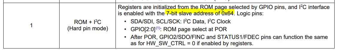
#define LMK_SLAVE_ADDRESS  0x78

void LMK05318_write(void);
void LMK05318_read_registers(void);


void LMK05318_read_registers(void)
{
    volatile uint8_t data_read=0;
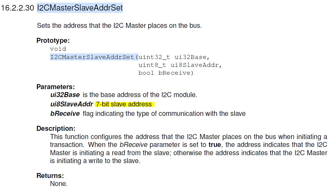
    I2CMasterSlaveAddrSet(I2C5_BASE, LMK_SLAVE_ADDRESS, false);
    I2CMasterDataPut(I2C5_BASE, 0x01);
    I2CMasterControl(I2C5_BASE, I2C_MASTER_CMD_BURST_SEND_START);
    //wait for MCU to finish transaction
     while(I2CMasterBusy(I2C5_BASE));
     I2CMasterDataPut(I2C5_BASE,0x3F); //low byte
      I2CMasterControl(I2C5_BASE, I2C_MASTER_CMD_BURST_SEND_FINISH);
     while(I2CMasterBusy(I2C5_BASE));
     while(I2CMasterBusy(I2C5_BASE));

     //specify that we are going to read from slave device
     I2CMasterSlaveAddrSet(I2C5_BASE, LMK_SLAVE_ADDRESS, true);
    //send control byte and read from the register we          //specified
     I2CMasterControl(I2C5_BASE, I2C_MASTER_CMD_SINGLE_RECEIVE);
    //wait for MCU to finish transaction
     while(I2CMasterBusy(I2C5_BASE));
    //return 1st byte pulled from the specified register
     data_read = I2CMasterDataGet(I2C5_BASE);
     GPIO_PORTK_DATA_R|=0x10;

}

void LMK05318_write(void)
{

  I2CMasterSlaveAddrSet(I2C5_BASE, (LMK_SLAVE_ADDRESS), false);
  while (I2CMasterBusy(I2C5_BASE));
  //I2CMasterBurstLengthSet (I2C5_BASE,3);
  I2CMasterDataPut(I2C5_BASE,0x01); //high byte
  I2CMasterControl(I2C5_BASE, I2C_MASTER_CMD_BURST_SEND_START);
  while (I2CMasterBusy(I2C5_BASE));
  while (I2CMasterBusy(I2C5_BASE));
  I2CMasterDataPut(I2C5_BASE, (0x3F)); //low byte
 I2CMasterControl(I2C5_BASE, I2C_MASTER_CMD_BURST_SEND_CONT);
 while (I2CMasterBusy(I2C5_BASE));
 while (I2CMasterBusy(I2C5_BASE));
  I2CMasterDataPut(I2C5_BASE, 0x18);//low byte
 I2CMasterControl(I2C5_BASE, I2C_MASTER_CMD_BURST_SEND_FINISH);
 while (I2CMasterBusy(I2C5_BASE));
 while (I2CMasterBusy(I2C5_BASE));

 }


int main(void)
{


    uint32_t ui32SysClock = MAP_SysCtlClockFreqSet((SYSCTL_XTAL_25MHZ |
                                               SYSCTL_OSC_MAIN | SYSCTL_USE_PLL |
                                               SYSCTL_CFG_VCO_480), 120000000);


         uint32_t sysCtlPeripheral = SYSCTL_PERIPH_I2C5;

         SysCtlPeripheralEnable(SYSCTL_PERIPH_I2C5);


         SysCtlPeripheralEnable(SYSCTL_PERIPH_GPIOA);
         SysCtlPeripheralEnable(SYSCTL_PERIPH_GPIOB);
         SysCtlPeripheralEnable(SYSCTL_PERIPH_GPIOK);
         GPIOPinTypeGPIOOutput(GPIO_PORTA_BASE, GPIO_PIN_2); //LED
         GPIOPinTypeGPIOOutput(GPIO_PORTK_BASE, GPIO_PIN_4); //LED


        GPIOPinConfigure(GPIO_PB4_I2C5SCL);
        GPIOPinConfigure(GPIO_PB5_I2C5SDA);
        GPIOPinTypeI2C(GPIO_PORTB_BASE, GPIO_PIN_5);
        GPIOPinTypeI2CSCL(GPIO_PORTB_BASE, GPIO_PIN_4);
        I2CMasterInitExpClk(I2C5_BASE, ui32SysClock, true);
        while(!SysCtlPeripheralReady(SYSCTL_PERIPH_I2C5));
        I2CMasterEnable(I2C5_BASE);

            GPIO_PORTA_AHB_DATA_R =0x00;
            GPIO_PORTC_AHB_DATA_R =0x00;
            GPIO_PORTK_DATA_R  =0x00;
            GPIO_PORTJ_AHB_DATA_R   =0x00;
            GPIO_PORTQ_DATA_R  =0x00;

       LMK05318_write();
       SysCtlDelay(10000);
       LMK05318_read_registers();

        while(1)
        {
         GPIO_PORTK_DATA_R|=LED_RED;
         SysCtlDelay(10000);
         GPIO_PORTA_AHB_DATA_R |=LED_BLU;
         SysCtlDelay(10000);

        }

}

  • Hi,

      Your capture is small. I can't really decipher. If you are using I2C5 then PB0 is supposed to be the SCL and the PB1 is the SDA. You PB1 (SCL) is just orange color. I can't tell what data is put on the bus. The PB0 is the I2C clock and it doesn't look like a clock to me. Please zoom in your capture and also make sure you have the pins connected correctly.

    I quickly glanced through the LMK05318 datasheet. The 7-bit slave address is 11001xx. The slave address can be 1100100 (0x64), 1100101 (0x65), 1100110 (0x66) or 1100111 (0x67). Where is the 0x78 coming from as you wrote in your code?

  • Thanks for the reply. I am sorry but the images below are get with the maximum zoom

    The first image is the writing sequence made with the EVM, the second the writing sequence taken with TM4C1294.(PB0 is SDA and PB1 is SCL)

    Concerning LMK05318 address. At the beginning I thought too, based on the datasheet, that the 7 bit address was 0x64. Then, when I saw the writing sequence with the analyzer I have put 0x78 which results in 0xF0 after the shifting . This is in line with what I see in TiCS Pro Software. When I send the command "Scan I2C bus", the program returns "Device found at 0x78".  I haven't touch the EVM default configuration . This is a topic I will discuss in the LMK05318 forum.

  • HI,

      The API expects you to enter the 7-bit slave address. This is the address before the shift. So you need to enter 0x64 as far as I can tell from the datasheet. If you think 0x78 may be the correct address then you should consult with the forum that support LMK05318 to confirm. I'm not familiar enough with it. 

      What is the EVM you are talking about? Is this a EVM for the LMK05318? Did you get it to work with the EVM?

       Do you have a custom board that you built with LMK05318 and the TM4C1294NCPDT that doesn't work or you are using the TM4C129 LaunchPad to interface with the LMK05318? I'm still not clear with your hardware setup.


  • At this stage, I am using the following EVM: LMK05318EVM. I haven't changed the default EVM power supply (VDD_DIG =3.3V and VDDO =1.8V) and communication settings.  The communication with TICS-Pro software works fine and I have managed to write different configurations.

    When I issue the I2C command with TM4C1294, I remove the jumpers SCL and SDA of JP20 and I connect a short  (around 4 cm) shielded cable . On the other side, the cable is connected with a custom board where TM4C1294 is soldered. On the custom board there aren't any other devices connected to  SCL and SDA signals

    The two boards have in common only the ground connection as the 3.3V power supply is delivered by two separate channels.

    On the custom board, the value of the pull-up resistors connected to SCL and SDA lines is 1k5

    According to the EVM schematics, when SDA and SCL jumpers are removed, there are no pull-up resistors connected to SCL and SDA signals. Therefore, when LMK05318 is connected with the TM4C1294, only the 1k5 resistors soldered on the custom board are connected to SDA and SCL signals.

  • Not sure if you check with the support forum for LMK05318 product at https://e2e.ti.com/support/clock-and-timing/f/48. In any case, i found the below address in the EVM's user's guide. It is 0x64. If you use 0x78 then it is wrong according to the user's guide although I'm not familiar with the LMK05318 to be sure if other addresses are allowed in different modes of operation. You will need to ask the Clock and Timing forum or read the user's guide on your own.

    Please also reference the example under C:\ti\TivaWare_C_Series-2.2.0.295\examples\boards\ek-tm4c1294xl-boostxl-senshub\humidity_sht21_simple. Although it is interfacing to a different I2C device, I think the functions I2CReadCommand() and I2CWriteCommand() could help you with your code. Especially look at the lines where it is first waiting for the master to be not busy before waiting for the master to be busy. 

        while(!MAP_I2CMasterBusy(I2C7_BASE))
        {
        }
        while(MAP_I2CMasterBusy(I2C7_BASE))
        {
        }

    //*****************************************************************************
    //
    // This function sends the specified command to the I2C slave device.
    //
    //*****************************************************************************
    void
    I2CWriteCommand(uint32_t ui32Command)
    {
        //
        // Set up the slave address with write transaction.
        //
        MAP_I2CMasterSlaveAddrSet(I2C7_BASE, SHT21_I2C_ADDRESS, false);
    
        //
        // Store the command data in I2C data register.
        //
        MAP_I2CMasterDataPut(I2C7_BASE, ui32Command);
    
        //
        // Start the I2C transaction.
        //
        MAP_I2CMasterControl(I2C7_BASE, I2C_MASTER_CMD_SINGLE_SEND);
    
        //
        // Wait until the I2C transaction is complete.
        //
        while(MAP_I2CMasterBusy(I2C7_BASE))
        {
        }
    }
    
    //*****************************************************************************
    //
    // This function will read three 8-bit data from the I2C slave. The first
    // two 8-bit data forms the humidity data while the last 8-bit data is the
    // checksum.  This function illustrates three different I2C burst mode
    // commands to read the I2C slave device.
    //
    //*****************************************************************************
    void
    I2CReadCommand(uint32_t * pui32DataRx)
    {
        //
        // Modify the data direction to true, so that seeing the address will
        // indicate that the I2C Master is initiating a read from the slave.
        //
        MAP_I2CMasterSlaveAddrSet(I2C7_BASE, SHT21_I2C_ADDRESS, true);
    
        //
        // Setup for first read.  Use I2C_MASTER_CMD_BURST_RECEIVE_START
        // to start a burst mode read.  The I2C master continues to own
        // the bus at the end of this transaction.
        //
        MAP_I2CMasterControl(I2C7_BASE, I2C_MASTER_CMD_BURST_RECEIVE_START);
    
        //
        // Wait until master module is done transferring.
        // The I2C module has a delay in setting the Busy flag in the register so
        // there needs to be a delay before checking the Busy bit.  The below loops
        // wait until the Busy flag is set, and then wait until it is cleared to
        // indicate that the transaction is complete.  This can take up to 633 CPU
        // cycles @ 100 kbit I2C Baud Rate and 120 MHz System Clock.  Therefore, a
        // while loop is used instead of SysCtlDelay.
        //
        while(!MAP_I2CMasterBusy(I2C7_BASE))
        {
        }
        while(MAP_I2CMasterBusy(I2C7_BASE))
        {
        }
    
        //
        // Read the first byte data from the slave.
        //
        pui32DataRx[0] = MAP_I2CMasterDataGet(I2C7_BASE);
    
        //
        // Setup for the second read.  Use I2C_MASTER_CMD_BURST_RECEIVE_CONT
        // to continue the burst mode read.  The I2C master continues to own
        // the bus at the end of this transaction.
        //
        MAP_I2CMasterControl(I2C7_BASE, I2C_MASTER_CMD_BURST_RECEIVE_CONT);
    
        //
        // Wait until master module is done transferring.
        //
        while(!MAP_I2CMasterBusy(I2C7_BASE))
        {
        }
        while(MAP_I2CMasterBusy(I2C7_BASE))
        {
        }
    
        //
        // Read the second byte data from the slave.
        //
        pui32DataRx[1] = MAP_I2CMasterDataGet(I2C7_BASE);
    
        //
        // Setup for the third read.  Use I2C_MASTER_CMD_BURST_RECEIVE_FINISH
        // to terminate the I2C transaction.  At the end of this transaction,
        // the STOP bit will be issued and the I2C bus is returned to the
        // Idle state.
        //
        MAP_I2CMasterControl(I2C7_BASE, I2C_MASTER_CMD_BURST_RECEIVE_FINISH);
    
        //
        // Wait until master module is done transferring.
        //
        while(!MAP_I2CMasterBusy(I2C7_BASE))
        {
        }
        while(MAP_I2CMasterBusy(I2C7_BASE))
        {
        }
        
        //
        // Note the third 8-bit data is the checksum byte.  It will be
        // left to the users as an exercise if they want to verify if the
        // checksum is correct.
        pui32DataRx[2] = MAP_I2CMasterDataGet(I2C7_BASE);
    }