This thread has been locked.

If you have a related question, please click the "Ask a related question" button in the top right corner. The newly created question will be automatically linked to this question.

Compiler/TMDSEMU110-U: CC3220SF SWD Programming

Part Number: TMDSEMU110-U
Other Parts Discussed in Thread: CC3220SF, UNIFLASH, CC3120

Tool/software: TI C/C++ Compiler

Hi,

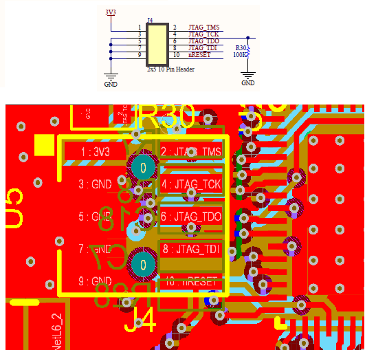
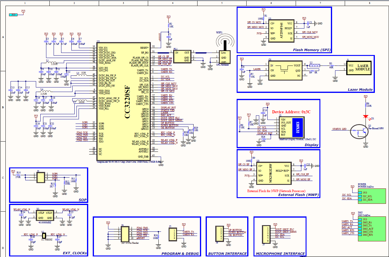
I proceeded at circuit side and I could successfully verified the my circuit over TSDSEMU110U (XDS110-USB) Programming device; But unfortunately I have not programmed device, yet. I got below error messages. So could you check device pinout which I asked at my last post at top and confirm pins' connections are True? 

[Start]

Execute the command:

%ccs_base%/common/uscif/dbgjtag -f %boarddatafile% -rv -o -S integrity

[Result]


-----[Print the board config pathname(s)]------------------------------------

C:\Users\Kemal-PC\AppData\Local\Texas Instruments\
CCS\ccs901\1\0\BrdDat\testBoard.dat

-----[Print the reset-command software log-file]-----------------------------

This utility has selected a 100- or 510-class product.
This utility will load the adapter 'jioxds110.dll'.
The library build date was 'Mar 25 2019'.
The library build time was '17:36:26'.
The library package version is '8.1.0.00007'.
The library component version is '35.35.0.0'.
The controller does not use a programmable FPGA.
The controller has a version number of '5' (0x00000005).
The controller has an insertion length of '0' (0x00000000).
This utility will attempt to reset the controller.
This utility has successfully reset the controller.

-----[Print the reset-command hardware log-file]-----------------------------

The scan-path will be reset by toggling the JTAG TRST signal.
The controller is the XDS110 with USB interface.
The link from controller to target is direct (without cable).
The software is configured for XDS110 features.
The controller cannot monitor the value on the EMU[0] pin.
The controller cannot monitor the value on the EMU[1] pin.
The controller cannot control the timing on output pins.
The controller cannot control the timing on input pins.
The scan-path link-delay has been set to exactly '0' (0x0000).

-----[Perform the Integrity scan-test on the JTAG IR]------------------------

This test will use blocks of 64 32-bit words.
This test will be applied just once.

Do a test using 0xFFFFFFFF.
Scan tests: 1, skipped: 0, failed: 0
Do a test using 0x00000000.
Scan tests: 2, skipped: 0, failed: 0
Do a test using 0xFE03E0E2.
Scan tests: 3, skipped: 0, failed: 0
Do a test using 0x01FC1F1D.
Scan tests: 4, skipped: 0, failed: 0
Do a test using 0x5533CCAA.
Scan tests: 5, skipped: 0, failed: 0
Do a test using 0xAACC3355.
Scan tests: 6, skipped: 0, failed: 0
All of the values were scanned correctly.

The JTAG IR Integrity scan-test has succeeded.

-----[Perform the Integrity scan-test on the JTAG DR]------------------------

This test will use blocks of 64 32-bit words.
This test will be applied just once.

Do a test using 0xFFFFFFFF.
Scan tests: 1, skipped: 0, failed: 0
Do a test using 0x00000000.
Scan tests: 2, skipped: 0, failed: 0
Do a test using 0xFE03E0E2.
Scan tests: 3, skipped: 0, failed: 0
Do a test using 0x01FC1F1D.
Scan tests: 4, skipped: 0, failed: 0
Do a test using 0x5533CCAA.
Scan tests: 5, skipped: 0, failed: 0
Do a test using 0xAACC3355.
Scan tests: 6, skipped: 0, failed: 0
All of the values were scanned correctly.

The JTAG DR Integrity scan-test has succeeded.

[End]

  • Hi,

    Please see the following thread for debugging under  the heading Incorrect SWD Header.

    software-dl.ti.com/.../ccsv7_debugging_jtag_connectivity_issues.html

    Thanks

  • Hi,

    My questions and my board's main schematic are at below. Could you please check schematic, my questions at below and give your answers, suggestions, please:

    Items Pin Associated Recommended Connection Situations and Questions
    XTAL 22 and 23 1. XTAL should be connected across 'Pin 22' and 'Pin 23'
    2. Provide load capacitors (6.2pF) at both the pins of the XTAL. This is based on TI board layout.
    3. Tuning of the load capacitance may be needed based on customer board layout.
    I see 40Mhz at Oscilloscope. It is OK.
    ANA DCDC IN 37 1. Should be connected to VBAT
    2. Provide de-coupling capacitor (4.7uF)
    There is No De-coupling capacitor = 4.7uF, 6.3V
    Could it be problem for running and programming?
    PA DCDC IN 39 1. Should be connected to VBAT
    2. Provide de-coupling capacitor (4.7uF)
    There is No De-coupling capacitor = 4.7uF, 6.3V
    Could it be problem for running and programming?
    DIG DCDC IN 44 1. Should be connected to VBAT
    2. Provide de-coupling capacitor (4.7uF)
    There is No De-coupling capacitor = 4.7uF, 6.3V
    Could it be problem for running and programming?
    VIO 54 and 10 1. Should be connected to VBAT
    2. Provide de-coupling capacitor (0.1uF) to each pin
    There is No De-coupling capacitor = 0.1uF, 10V
    Could it be problem for running and programming?
    Flash_SPI 11, 12, 13 and 14 1. Please connect CS# (Flash) to device 'Pin 14', DOUT (Flash) to DIN (Dev Pin 13), DIN (Flash) to DOUT (Dev Pin 12) and Clock (Flash) to CLK (Dev Pin 11)
    2. Provide 0.1uF de-coupling capacitor for the supply of the flash
    3. 32Mbit part is recommended
    4. Add 100K pull up resistor on CS# (Pin #14) line
    Pin# 11, 12, 13, 14 (Flash SPI lines) Pins connected to Macronix  MX25R3235F on my circuit. Should MX25R3235F be pre-programmed before CC3220SF's first programming?

    SOP 21, 34 and 35 1. 100K pull down resistor to GND should be provided to pins 34 and 35
    2. 2.7k pull down resistor to GND should be provided to Pin 21
    3. Pull up to VBAT option should be provided at SOP0 (pin #35). This is required if user chooses to use SWD debug mode instead of 4 wire JTAG
    4. Pull up to VBAT option should be provided at SOP2 (pin #21). This is required for entering the UART load mode for flashing FW, application, certificate etc.

    Note : The SOP0 and SOP1 lines would be driven low by the device in hibernate state. This can lead to higher leakage in case a pull-up resistor is added on this line. Hence it is recommended to keep pull-down on these pins on final product. For SWD mode, the line can be pulled high by emulator/debugger.
    Which Mode [xxx] I should set for UART Programming? As I defined my Uart pins are My UART0_TX (Pin3 of CC3220SF), My UART0_RX (Pin4 of CC3220SF) on my board.
      55, 57, 32, 21 1. The following pins should be brought out to test points for flash programming.
    Pin #      Description
    57          RX
    55          TX
    32          nRESET
    21          SOP2
    2. For flash programming, SOP2 should be held high before nRESET goes high.
    3. Ensure that while programming, the RX (pin #57) and TX (pin #55) are NOT driven by any other circuit on the board.
    For Serial Debug (Programming), My UART0_TX (Pin3 of CC3220SF), My UART0_RX (Pin4 of CC3220SF) are connected to external connector and I want to do programming over these pins. When I set these pins as UART at CCS Library side, I guess I could do programming over Pins 3 and 4. I will do programming on Debug mode of CCS and burning (Serial Aux) from UniFlash.
        The following pins need to be brought on to a header,connector or  Test point to be able to access the serial flash for  In-circuit programming
    Pin# 11, 12, 13, 14 (Flash SPI lines)
    Pin# 32 (nRESET)
    Vcc, GND

    Ensure that the programmer can hold the CC3120 device in RESET mode while accessing the s-flash.
    Pin# 11, 12, 13, 14 (Flash SPI lines) Pins connected to Macronix  MX25R3235F on my circuit. Should MX25R3235F be pre-programmed before CC3220SF's first programming?
  • Hi,

    Sorry for the delay on this. I have forwarded this to the HW team to confirm the connections in the schematic.

    Thanks for your patience.

    Regards,

  • Hi,

    I need fast return and solution, please. Also I connected 37, 39, 44, 54, 10 pins to 3V3 directly using 0R instead of capacitors. I see 40Mhz on Oscilloscope. Please direct these details to HW Team. I am waiting HW Team's answer.

    Thanks.

  • Hi Kemal,

    I reviewed your schematic. Here are my notes:

    1. For CC3220SF, pin47 should not be connected to VBAT. See reference design.
    2. The UART pins 55 and 57 should be used for programming. Add a 100k pull up resistor to both signals. Use SOP configuration 010 for UART programming. See Section 6.8 in the CC3220 datasheet.
    3. The CC3220SF's engine area should follow our reference design exactly to ensure that it works properly. This includes the decoupling caps and other components on the power rail and DC-DC pins.
    4. The external flash does not have to be pre-programmed. 

    The SOP config must be set to 001 before powering the device on to use SWD. Also ensure that the device is set to development mode via Uniflash to use JTAG/SWD. The JTAG is disconnected due to security reasons when the device is in production mode. Did you already try or check this?

    BR,

    Seong

  • Thanks. When I revise UART-1 Port as 55 & 57 and added pullup Resistor to these pins, My programming problem was resolved. Also, I added decoupling resistors, But I think pull up resistors was solved issue.