This thread has been locked.

If you have a related question, please click the "Ask a related question" button in the top right corner. The newly created question will be automatically linked to this question.

MSP432P401R: ADC Interrupt ISR compared to ADC Trigger

Part Number: MSP432P401R

Why does the ADC ISR only run every other ADC Trigger which is the Timer A0_1 source.

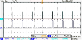
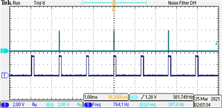
In the picture below

CH1 is the Timer A0_1 out which is the ADC trigger source and CH2 is an output bit togged on and off inside the ADC ISR.

Code is shown below.

#include "msp.h"

uint16_t resultsBuffer[2];

void main(void){

    WDT_A->CTL = WDT_A_CTL_PW | WDT_A_CTL_HOLD;

    P5->SEL1 |= BIT5 | BIT4; // Set P5.5 as ADC input A0 and P5.4 as ADC input A1
    P5->SEL0 |= BIT5 | BIT4; // Set P5.5 as ADC input A0 and P5.4 as ADC input A1

    // initialize P1.0  for Output
    P1->DIR  |= 0b00000001;  // Set P1.0 Output pin
    P1->OUT  &= ~1;          /* turn off P1.0 */

    // initialize P2.4 and make it a timer output
    P2->DIR  |= 0b00010000;  // Set P2.4 as an Output pin
    P2->SEL0 |= 0b00010000;  // Set P2.4 as Primary function Timer_A0_C1  CCR0 Output

    // initialize P4.2 and make it a timer output
    P4->DIR  |= 0b00000100;  // Set P4.2 as an Output pin
    P4->SEL0 |= 0b00000100;  // Set P4.2 as Primary function ACLK

    CS->KEY = CS_KEY_VAL;
    CS->CTL1 |= CS_CTL1_SELA_2;
    CS->KEY = 0;

    ADC14->CTL0 &= ~ADC14_CTL0_ENC; // Reset ENC bit for configuration
    //Timer_A0 output 1 trigger, Sampling timer is the source of sampling signal, multi channel-repeated conversion mode, Sample and hold time is 8 ADC clock cycles, ADC14 on
    ADC14->CTL0 = ADC14_CTL0_SHS_1 | ADC14_CTL0_SHP | ADC14_CTL0_CONSEQ_3 | ADC14_CTL0_SHT0_1 | ADC14_CTL0_ON;
    ADC14->MCTL[0] = ADC14_MCTLN_VRSEL_0 | ADC14_MCTLN_INCH_0; // Vcc - Vss references, input channel A0, End of sequence
    ADC14->MCTL[1] = ADC14_MCTLN_VRSEL_0 | ADC14_MCTLN_INCH_1 | ADC14_MCTLN_EOS; // Vcc - Vss references, input channel A1, End of sequence
    ADC14->IER0 = ADC14_IER0_IE1; // ADC interrupt enabled for ADC14->MEM[1]

    ADC14->CTL0 |= ADC14_CTL0_ENC; // Start conversion-software trigger

    TIMER_A0->CCR[0] = 42;  // PWM period
    TIMER_A0->CCR[1] = 4; // CCR1 PWM duty cycle
    TIMER_A0->CCTL[1] = TIMER_A_CCTLN_OUTMOD_6; // CCR1 set/reset
    TIMER_A0->CTL = TIMER_A_CTL_TASSEL_1 | TIMER_A_CTL_MC_1 |  TIMER_A_CTL_CLR; // ACLK, Up mode, Clear TAR

    NVIC->ISER[0] = 0x01000000; // ADC14 interrupt is enabled in NVIC
    __enable_irq(); // All interrupts are enabled

    SCB->SCR |= SCB_SCR_SLEEPONEXIT_Msk; // Sleep on exit
    __sleep(); // enter LPM0
}

// ADC14 interrupt service routine
void ADC14_IRQHandler(void){
        P1->OUT |= 1;             /* turn on P1.0 */
    if (ADC14->IFGR0 & ADC14_IFGR0_IFG1){
        resultsBuffer[0] = ADC14->MEM[0];
        resultsBuffer[1] = ADC14->MEM[1];
        P1->OUT &= ~1;            /* turn off P1.0 */
        __no_operation();}
}

  • With CONSEQ=3 and MSC=0, you get one conversion per trigger [Ref TRM (SLAU356I) Fig 22-10]. Since the interrupt only happens on the last (second) channel in the sequence you get one ADC interrupt every 2x conversions/triggers. You could:

    1) Enable the interrupt for both channels. This will give you low latency but (still) won't give you burst behavior.

    2) Use CONSEQ=1 and MSC=1. This will give you burst behavior -- 2x conversions per trigger -- but you will need to toggle (low then high) ENC between bursts (in the ISR, probably). [Ref TRM Fig 22-8]

    [Edit: I forgot option

    3) Decide that the current behavior is fine, and don't change anything. (Maybe double the trigger frequency.) Sometimes you don't care about bursting, since the channels are unrelated, and the ENC thing is a particular headache if you want to do DMA.]

  • Thanks I tried using your 2) suggestion

    Use CONSEQ=1 and MSC=1

    The updated code is

    #include "msp.h"
    
    uint16_t resultsBuffer[2];
    
    void main(void){
    
        WDT_A->CTL = WDT_A_CTL_PW | WDT_A_CTL_HOLD;
    
        P5->SEL1 |= BIT5 | BIT4; // Set P5.5 as ADC input A0 and P5.4 as ADC input A1
        P5->SEL0 |= BIT5 | BIT4; // Set P5.5 as ADC input A0 and P5.4 as ADC input A1
    
        // initialize P1.0  for Output
        P1->DIR  |= 0b00000001;  // Set P1.0 Output pin
        P1->OUT  &= ~1;          /* turn off P1.0 */
    
        // initialize P2.4 and make it a timer output
        P2->DIR  |= 0b00010000;  // Set P2.4 as an Output pin
        P2->SEL0 |= 0b00010000;  // Set P2.4 as Primary function Timer_A0_C1  CCR0 Output
    
        // initialize P4.2 and make it a timer output
        P4->DIR  |= 0b00000100;  // Set P4.2 as an Output pin
        P4->SEL0 |= 0b00000100;  // Set P4.2 as Primary function ACLK
    
        CS->KEY = CS_KEY_VAL;
        CS->CTL1 |= CS_CTL1_SELA_2;
        CS->KEY = 0;
    
        ADC14->CTL0 &= ~ADC14_CTL0_ENC; // Reset ENC bit for configuration
        //Timer_A0 output 1 trigger, Sampling timer is the source of sampling signal, multi channel-repeated conversion mode, Sample and hold time is 8 ADC clock cycles, ADC14 on
    
    //    ADC14->CTL0 = ADC14_CTL0_SHS_1 | ADC14_CTL0_SHP | ADC14_CTL0_CONSEQ_3 | ADC14_CTL0_SHT0_1 | ADC14_CTL0_ON;
    
        ADC14->CTL0 = ADC14_CTL0_SHS_1 | ADC14_CTL0_SHP | ADC14_CTL0_CONSEQ_1 | ADC14_CTL0_SHT0_1 | ADC14_CTL0_ON | ADC14_CTL0_MSC;
    
        ADC14->MCTL[0] = ADC14_MCTLN_VRSEL_0 | ADC14_MCTLN_INCH_0; // Vcc - Vss references, input channel A0, End of sequence
        ADC14->MCTL[1] = ADC14_MCTLN_VRSEL_0 | ADC14_MCTLN_INCH_1 | ADC14_MCTLN_EOS; // Vcc - Vss references, input channel A1, End of sequence
        ADC14->IER0 = ADC14_IER0_IE1; // ADC interrupt enabled for ADC14->MEM[1]
    
        ADC14->CTL0 |= ADC14_CTL0_ENC; // Start conversion-software trigger
    
        TIMER_A0->CCR[0] = 42;  // PWM period
        TIMER_A0->CCR[1] = 4; // CCR1 PWM duty cycle
        TIMER_A0->CCTL[1] = TIMER_A_CCTLN_OUTMOD_6; // CCR1 set/reset
        TIMER_A0->CTL = TIMER_A_CTL_TASSEL_1 | TIMER_A_CTL_MC_1 |  TIMER_A_CTL_CLR; // ACLK, Up mode, Clear TAR
    
        NVIC->ISER[0] = 0x01000000; // ADC14 interrupt is enabled in NVIC
        __enable_irq(); // All interrupts are enabled
    
        SCB->SCR |= SCB_SCR_SLEEPONEXIT_Msk; // Sleep on exit
        __sleep(); // enter LPM0
    }
    
    // ADC14 interrupt service routine
    void ADC14_IRQHandler(void){
            P1->OUT |= 1;             /* turn on P1.0 */
            ADC14->CTL0 &= ~ADC14_CTL0_ENC; // Reset ENC bit for configuration
            if (ADC14->IFGR0 & ADC14_IFGR0_IFG1){
            resultsBuffer[0] = ADC14->MEM[0];
            resultsBuffer[1] = ADC14->MEM[1];
            P1->OUT &= ~1;            /* turn off P1.0 */
            ADC14->CTL0 |= ADC14_CTL0_ENC; // Start conversion-software trigger
            __no_operation();}
    }
    

    Now the ADC ISR is happening on every Timer trigger.

    See scope shot below

    CH1 is the Timer A0_1 out which is the ADC trigger source and CH2 is an output bit togged on and off inside the ADC ISR.


    The code I posted has been modified a lot from the original, but to give credit to the original example, it came from

    the Book: Programmable Microcontrollers: Application On The MSP432 LaunchPad.  Starting Example code was Listing 8.10