This thread has been locked.

If you have a related question, please click the "Ask a related question" button in the top right corner. The newly created question will be automatically linked to this question.

TMS320F280025: TMS320f28002x UL60730 self-test Library

Part Number: TMS320F280025
Other Parts Discussed in Thread: C2000WARE, AFE031, CCSTUDIO, , SFRA

Hi

I am going to apply UL60730 for application with TMS320F28002x MCU. However, I can't find any library to the MCU series. Please advice how to get the library and the document.

BR

HK Woo

  • The device safety manual is here if you haven't seen it already: https://www.ti.com/lit/pdf/spruit5

    There is a diagnostic library for the F28002x in C2000Ware. Look for it under libraries/diagnostic/f28002x.

    Whitney

  • I followed your information to download the document "safety manual" and review it. It seems to be a document describe the feature of the MCU only. It doesn't show us how to implement the self test.

    I download "Diag_Lib_TMS320F28002x_Users_Guide" under C2000Ware/libraries/diagnostic/f28002x/docs and import an example "sdl_ex_ram_parity_test".

    Do TI have a document to explain the example? It is because I can't find function explanation e.g. MemCfg_setTestMode...

    BR

    HK Woo

  • The safety manual provides a good summary of the different diagnostics and mechanisms, but it's still helpful to look them up in the technical reference manual for additional details.

    There is a User's Guide for the diagnostic library although it is generated from the comments at the top of the main .c file in the project, so you can just read those. Most of the functions called in the examples (like MemCfg_setTestMode) are from the Driverlib. You can find the Driverlib API reference guide here or in C2000Ware under device_support/f28002x/docs/html/index.html.

    Whitney

  • Whitney

    I still don't understand the process of self-test process for the MCU. I locate in Hong Kong. Is there are any chance to have zoom call with TI support to discuss it. Our project is running out of time. Need TI support.

    BR

    HK Woo

  • What aspects of the process are giving you trouble? Are you having trouble identifying which tests need to be run? Or understanding how to configure the device to run them? Or something else?

    Whitney

  • Hi Whitney

    I am stucking @ 2 area. RAM and Flash testing in IEC60730 requirement.

    I am using TI PLC IC AEF031 and its compiled library fsk_corr_detect_lib_eabi.lib which is provided by TI.

    RAM testing.

    1.According to IEC60730, it is necessary to do RAM DC fault which related to the lib. However, I don't know that actual address of the variable using by the library.

    2.If we are going to review the source code of the library. it is too risky to modify the code by our own.

    Flash testing.

    1. Cannot find any document/example code to read the content of flash for checksum checking

    2. How to reserve a small portion of flash as EEPORM

    3. How to burn a checksum value to item 2 if flash simulates EEPORM during firmware burning process. For example,  store a checksum data to .out or .hex so that it is not necessary to write communication function to send a checksum to MCU and then write it to simulated EEPORM.

    BR

    HK Woo

  • Hi Whitney

    I got an information from safety agency. Some requirement for IEC60730 application, it is necessary to check  register as below

    1. ACC, P, XT, XAR3-XAR7, PC, RPC, ST0, ST1, DP, SP, IER, IFR, DBGIER. Test algorithm can be write 55H and read out if 55H; write AAH and read out if AAH 

    2. Need to check all RAM any DC fault

    For item 1, I found a demo code f28002x_test_application. It seems that an API call STL_CPU_REG_checkCPURegisters() will check all these CPU Register.

    I have a question as below

    a. Does the API will affect more program flow. It is because there is an ISR running @ 300K Hz to sample the PLC signal from TI PLC chip AFE031.

    b. What is total execution time of the API? The reason to have it is to prevent overflow due to item a. In the demo code sta_tests.c

                DINT;
    #if STA_UTIL_PROFILE
                STA_Util_startProfiler(CPUTIMER1_BASE);
    #endif

                uint16_t returnVal =
                        STL_CPU_REG_checkCPURegisters(STA_Tests_injectError);

    #if STA_UTIL_PROFILE
                uint32_t cycleCount = STA_Util_stopProfiler(CPUTIMER1_BASE);
                STA_Tests_cycleCounts[STA_CPU_REG] = cycleCount;

    STA_Tests_cycleCounts[STA_CPU_REG] is 686 from CCStudio expressions windows. Is it mean that it takes 6.86us

    Furthermore, any problem if I delete above codes in RED. It seems that it is for determine the execution time only, is it right?

    c. Could you explain to me why the input parameter of the API is bool True or False. I don't understand the explanation from the document "Diag_Lib_TMS320F28002x"

    For item 2, I am studying the demo code sdl_ex_ram_ecc_parity_test, is it correct?


  • Were you able to request access to the fsk_corr_detect_lib_eabi.lib source code?

    On the subject of RAM testing, the SRAMs already have either ECC or Parity enabled at reset in the hardware (SRAM1 and SRAM2 in the safety manual). sdl_ex_ram_ecc_parity_test demonstrates how to perform a software test of the functionality of the ECC/Parity functionality (SRAM13/SRAM14). To perform a more proactive test of of the SRAM, you can take a look at the STL_March module in the library that goes through a given memory range and writes patterns to the RAM to check for stuck bits.

    Flash is similar in that it has hardware ECC for which a test of the diagnostic can be performed (sdl_ex_flash_ecc_test example). As for doing a CRC check, you can use the STL_CRC functions in the library. The f28002x_test_application demonstrates how to use the functions by doing a check on a small portion of the OTP, but you can use it on other memories. There's a document here on how to have the linker generate CRC tables for you:
    software-dl.ti.com/.../appnote-perform_crc_check.html

    You are correct that the STL_CPU_REG can do a check of the CPU registers. The parameter is for injecting an error into the test to make it fail on purpose so you can test that you're application is reacting properly to the error.

    Your understanding of the profiling functions is correct. The value it returns is in clock cycles, so assuming a SYSCLK of 100MHz, 6.68us is correct. You do not have to keep the profiling functions in your code. They are just there for the convenience of doing some benchmarking of the functions.

    Whitney

  • Hi Whitney

    For API STL_CPU_REG_checkCPURegisters(), I still don't understand. If I want to check CPU register which is ok or not. What is parameter should be used "ture" or "false"?. It is my understanding as below

    Case 1

    x = STL_CPU_REG_checkCPURegisters(false);

    x should be CPU_REG_PASS if register is no problem otherwise CPU_REG_FAIL is reture;

    Case 2

    x = STL_CPU_REG_checkCPURegisters(true);

    x should be CPU_REG_FAIL if registers are no problem otherwise CPU_REG_PASS is return ;

    For self-test setup, it is necessary to have below codes

        EALLOW;
        HWREGH(NMI_BASE + NMI_O_FLGCLR) = 0xFFFF;
        HWREGH(NMI_BASE + NMI_O_CFG) |= NMI_CFG_NMIE;
        EDIS;

    I have question, is it necessary to re-configure it to normal mode or just keep it all the time for example

    main()

    .....

        EALLOW;
        HWREGH(NMI_BASE + NMI_O_FLGCLR) = 0xFFFF;
        HWREGH(NMI_BASE + NMI_O_CFG) |= NMI_CFG_NMIE;
        EDIS;

       for(;;)

       {

            .....

             my application code;

            .....

            if (need to do CPU register test)

           {

                 DINT;

    /* Or put above code in RED here ???????*/

                 x = STL_CPU_REG_checkCPURegisters(true);

                if (x == CPU_REG_FAIL)

               {

                    my code;

               }

    /* Do we need to re-configure NMI_BASE to other mode, show that my application running as normal operation at here, if it necessary what is the code.*/

               EINT;

          }

    ISR(vode)

    {

          my code;

    }

    -.For RAM/Flash checking, I am still reviewing the code.

    -.For fsk_corr_detect_lib_eabi.lib. I received a source via TI website. I don't know TI send me a correct version or not. It is because TI publish the lib in website is not for EABI format.

    BR

    HK Woo

  • For normal operation, you would leave the error injection parameter false (case 1). The option to inject an error is just there for you to test how your system handles an error if one were to be detected.

    You shouldn't need to do anything with the NMI to run the STL_CPU_REG tests. The STL_CPU_REG test won't generate an NMI, even if a fault is detected. You probably don't need that line to write to NMIE in your application at all. When running standalone the boot ROM enables the NMI and when running in debug mode, the GEL file does it, assuming you're using the CCS default.

    I'll investigate whether or not there were any code changes to the fsk_corr_detect_lib_eabi.lib source to allow it to be built for EABI.

    Whitney

  • Hi Whitney

    Thanks for your information. I finished a code on CPU register. I am going to start a code for RAM. According to Safety agency, it is required to check entire portion of RAM. I can't from the start address and end address of RAM. Could you provide to me?

    I am thinking to use STL_March_testRAMCopy and STL_March_checkErrorStatus for RAM DC DC Fault

    Below is my idea on coding

    DINT;    

    STL_March_testRAMCopy ( STL_MARCH_PATTERN_ONE,  0x0000, 7,  0xFFFFF);

    EINT;
    uint16 returnVal STL_March_checkErrorStatus();

    if (returnVal != STL_MARCH_PASS) ErrorFound

    It is correct and Could you explains what is STL_MARCH_PATTERN_ONE,STL_MARCH_PATTERN_TWO....

    Thanks a lot

  • There's a table in the datasheet the shows the addresses and sizes of all the different RAMs. In the latest version of the data sheet, it's in section 8.3.1: https://www.ti.com/lit/pdf/sprsp45

    Those functions will work. If you're able to run the test before you call _c_int00 to initialize the variables in RAM, you could use STL_March_testRAM which is quicker because it doesn't do a save and restore to the memory. I've seen other customers have success with that approach, but if the execution time isn't an issue or you plan on running the test periodically in small sections at a time, what you have is fine.

    There's a document here that explains a little bit more about what the patterns are for: https://www.ti.com/lit/pdf/spracb9

    The recommendation is to cycle through them if you can to improve your diagnostic coverage, but it's not strictly necessary.

    Whitney

  • Whitney

    IEC requires to run ram test periodically and hence I need to use STL_MarchRAMCopy.I have question, is it necessary to do any init function before run my code.

  • Can you elaborate? Do you specifically mean before you run STL_March_testRAMCopy? If that's whatyou mean, no, there is no init function for STL_March_testRAMCopy. As long as it has read/write access to the RAM being tested, it should be ready to go.

    Whitney

  • Hi Whitney

    I reviewed a code in project f28002x_test_application sta_tests.c

            case STA_MARCH_COPY:
            {
                uint32_t originalValue;
                uint16_t index;

                //
                // Filling STA_User_marchTestData to make the copy easier to
                // observe.
                //
                for(index = 0; index < STA_USER_MARCH_DATA_SIZE; index++)
                {
                    STA_User_marchTestData[index] = index;
                }

                //
                // Clear RAM error status flags.
                //
                MemCfg_clearUncorrErrorStatus(MEMCFG_UCERR_CPUREAD |
                                              MEMCFG_UCERR_DMAREAD);
                MemCfg_clearCorrErrorStatus(MEMCFG_CERR_CPUREAD);

                //
                // Initialize the inject error handle for stl_march.
                //
                STA_User_initMarch();

                //
                // Inject an error in the memory.
                //
                if(STA_Tests_injectError)
                {
                    //
                    // Cause a single bit error in M0 (ECC, correctable)
                    //
                    originalValue = HWREG(STA_User_marchErrorObj.address);
                    STA_User_marchErrorObj.testMode = MEMCFG_TEST_WRITE_DATA;
                    STA_User_marchErrorObj.xorMask = 0x00000001U;
                    STL_March_injectError(STA_User_marchErrorHandle);
                }

    #if STA_UTIL_PROFILE
                STA_Util_startProfiler(CPUTIMER1_BASE);
    #endif

                STL_March_testRAMCopy(STL_MARCH_PATTERN_ONE,
                                      (uint32_t)STA_User_marchTestData,
                                      (STA_USER_MARCH_DATA_SIZE / 2U) - 1U,
                                      (uint32_t)STA_User_marchTestDataCopy);

    #if STA_UTIL_PROFILE
                uint32_t cycleCount = STA_Util_stopProfiler(CPUTIMER1_BASE);
                STA_Tests_cycleCounts[STA_MARCH_COPY] = cycleCount;
    #endif

    There is an instruction  STA_User_initMarch() which I don't know I need to_a use it or not. In the instruction             STL_March_testRAMCopy(STL_MARCH_PATTERN_ONE,
                                      (uint32_t)STA_User_marchTestData,
                                      (STA_USER_MARCH_DATA_SIZE / 2U) - 1U,
                                      (uint32_t)STA_User_marchTestDataCopy);

    Why start and copy address are name of variable with array index? It is expected that it is address of RAM e.g. 0x0000 something like that.

    Actually, I am going to check entire RAM in small section as what you said.

    My code likes and use M0 as example

    uint32 strat_address = 0x000000;

    main()

    {

         if (ramCheck)

        {       

              DINT;    

              STL_March_testRAMCopy ( STL_MARCH_PATTERN_ONE,  start_address, 7,  0xFFFFF); // 7 is represented 8 RAM address need to check
              uint16 returnVal STL_March_checkErrorStatus();

              if (returnVal != STL_MARCH_PASS) ErrorFound;

              start_address = start_address + 8;

             if (start_address == 0x3FF) start_address = 0x0000;

              ramCheck = false;

        }

        my main loop programm code....

    }

    timer_isr()

    {

        ramCheck = true;

    }

    Furthermore, I plan to reserve a RAM for copy address which is using as temporary storage for   STL_March_testRAMCopy. How to do it in link file or any other method?

    Actually the code is used for checking entire RAM section. Is it correct code?

    In the document https://www.ti.com/lit/pdf/sprsp45 section 8.3.1 I still have a question

    Take M0 as example, 1K x 16 from 0x000 to 0x3FF. what is meaning of 16.  Is it 16 bits. If my code STL_March_testRAMCopy ( STL_MARCH_PATTERN_ONE,  0x0000, 7,  0xFFFFF); Is it mean that the API will check address from 0x0000 to 0x0007 total 8 in length.

    If some of my program running in RAM, is there are problem to run the RAM testing.

    Furthermore, please find below in link file for my project using TMS320F280025. It seems that the address is different from the document mentioned in Section 8.3.1

    MEMORY
    {
       BEGIN               : origin = 0x080000, length = 0x000002
       BOOT_RSVD        : origin = 0x00000002, length = 0x00000126
       RAMM0               : origin = 0x00000128, length = 0x000002D8
       RAMM1            : origin = 0x00000400, length = 0x000003F8     /* on-chip RAM block M1 */
    // RAMM1_RSVD       : origin = 0x000007F8, length = 0x00000008 /* Reserve and do not use for code as per the errata advisory "Memory: Prefetching Beyond Valid Memory" */

    /* RAMLS4           : origin = 0x0000A000, length = 0x00000800
       RAMLS5           : origin = 0x0000A800, length = 0x00000800
       RAMLS6           : origin = 0x0000B000, length = 0x00000800
       RAMLS7           : origin = 0x0000B800, length = 0x00000800*/

       /* Combining all the LS RAMs */
       RAMLS4567        : origin = 0x0000A000, length = 0x00002000
       RAMGS0           : origin = 0x0000C000, length = 0x000007F8
    // RAMGS0_RSVD      : origin = 0x0000C7F8, length = 0x00000008 /* Reserve and do not use for code as per the errata advisory "Memory: Prefetching Beyond Valid Memory" */


    //  FLASHBANK1       : origin = 0x00080000, length = 0x0000FFF0
    //  FLASH_BANK1_RSVD : origin = 0x0008FFF0, length = 0x00000010 /* Reserve and do not use for code as per the errata advisory "Memory: Prefetching Beyond Valid Memory" */
       BOOTROM          : origin = 0x003F0000, length = 0x00008000
       BOOTROM_EXT      : origin = 0x003F8000, length = 0x00007FC0
       RESET            : origin = 0x003FFFC0, length = 0x00000002
       /* Flash sectors */
       /* BANK 0 */
       FLASH_BANK0_SEC0  : origin = 0x080002, length = 0x000FFE    /* on-chip Flash */
       FLASH_BANK0_SEC1  : origin = 0x081000, length = 0x001000    /* on-chip Flash */
       FLASH_BANK0_SEC2  : origin = 0x082000, length = 0x001000    /* on-chip Flash */
       FLASH_BANK0_SEC3  : origin = 0x083000, length = 0x001000    /* on-chip Flash */
       FLASH_BANK0_SEC4  : origin = 0x084000, length = 0x001000    /* on-chip Flash */
       FLASH_BANK0_SEC5  : origin = 0x085000, length = 0x001000    /* on-chip Flash */
       FLASH_BANK0_SEC6  : origin = 0x086000, length = 0x001000    /* on-chip Flash */
       FLASH_BANK0_SEC7  : origin = 0x087000, length = 0x001000    /* on-chip Flash */
       FLASH_BANK0_SEC8_9_10  : origin = 0x088000, length = 0x003000    /* on-chip Flash */
       //FLASH_BANK0_SEC8  : origin = 0x088000, length = 0x001000    /* on-chip Flash */
       //FLASH_BANK0_SEC9  : origin = 0x089000, length = 0x001000    /* on-chip Flash */
       //FLASH_BANK0_SEC8_9: origin = 0x088000, length = 0x002000    /* on-chip Flash */
       //FLASH_BANK0_SEC10 : origin = 0x08A000, length = 0x001000    /* on-chip Flash */
       FLASH_BANK0_SEC11 : origin = 0x08B000, length = 0x001000    /* on-chip Flash */
       FLASH_BANK0_SEC12 : origin = 0x08C000, length = 0x001000    /* on-chip Flash */
       FLASH_BANK0_SEC13 : origin = 0x08D000, length = 0x001000    /* on-chip Flash */
       FLASH_BANK0_SEC14 : origin = 0x08E000, length = 0x001000    /* on-chip Flash */
       FLASH_BANK0_SEC15 : origin = 0x08F000, length = 0x000FF0    /* on-chip Flash */
    // FLASH_BANK0_SEC15_RSVD     : origin = 0x08FFF0, length = 0x000010  /* Reserve and do not use for code as per the errata advisory "Memory: Prefetching Beyond Valid Memory" */

    }


    SECTIONS
    {
       codestart        : > BEGIN, ALIGN(8)
       .text            : >> FLASH_BANK0_SEC2 | FLASH_BANK0_SEC3 | FLASH_BANK0_SEC4 | FLASH_BANK0_SEC5,   ALIGN(8)
       .cinit           : > FLASH_BANK0_SEC1,  ALIGN(8)
       .switch          : > FLASH_BANK0_SEC1,  ALIGN(8)
       .reset           : > RESET,                  TYPE = DSECT /* not used, */

       .stack           : > RAMM1

       .init_array      : > FLASH_BANK0_SEC1,  ALIGN(8)
       .bss             : > RAMLS4567
       .bss:output      : > RAMLS4567
       .bss:cio         : > RAMGS0
       .const           : > FLASH_BANK0_SEC1,  ALIGN(8)
       .data            : > RAMLS4567
       .sysmem          : > RAMLS4567

        ramgs0 : > RAMGS0

       /*  Allocate IQ math areas: */
       IQmath           : > RAMLS4567
       IQmathTables     : > RAMLS4567

       fsk_corr_lib_data : > RAMLS4567

       GROUP
       {
           .TI.ramfunc
           {
               -l sfra_f32_tmu_eabi.lib
           }
           ramfuncs

       } LOAD = FLASH_BANK0_SEC6,
             RUN = RAMLS4567,
             LOAD_START(RamfuncsLoadStart),
             LOAD_SIZE(RamfuncsLoadSize),
             LOAD_END(RamfuncsLoadEnd),
             RUN_START(RamfuncsRunStart),
             RUN_SIZE(RamfuncsRunSize),
             RUN_END(RamfuncsRunEnd),
             ALIGN(4)

    /*
      .TI.ramfunc      : LOAD = FLASH_BANK0_SEC1,
                      RUN = RAMGS0,
                      LOAD_START(RamfuncsLoadStart),
                      LOAD_SIZE(RamfuncsLoadSize),
                      LOAD_END(RamfuncsLoadEnd),
                      RUN_START(RamfuncsRunStart),
                      RUN_SIZE(RamfuncsRunSize),
                      RUN_END(RamfuncsRunEnd),
                      ALIGN(8)
    */
        SFRA_F32_Data    : > RAMLS4567, ALIGN = 64

        FPUmathTables    : > FLASH_BANK0_SEC11


        //.scratchpad      : > RAMLS4567
        //controlVariables : > RAMLS4567

        GROUP
        {
            isrcodefuncs
            dclfuncs
        }    LOAD = FLASH_BANK0_SEC8_9_10,
             RUN =  RAMLS4567,
             LOAD_START(isrcodefuncsLoadStart),
             LOAD_SIZE(isrcodefuncsLoadSize),
             LOAD_END(isrcodefuncsLoadEnd),
             RUN_START(isrcodefuncsRunStart),
             RUN_SIZE(isrcodefuncsRunSize),
             RUN_END(isrcodefuncsRunEnd),
             ALIGN(4)


    }

    BR

    HK Woo


    HK

  • Dear 

    The domain expert in this area is out of the office at the moment and will be returning on July 21.  Your detailed responses will be delayed. 

    In regards to your question below:

    There is an instruction  STA_User_initMarch() which I don't know I need to_a use it or not. In the instruction             STL_March_testRAMCopy(STL_MARCH_PATTERN_ONE,
                                      (uint32_t)STA_User_marchTestData,
                                      (STA_USER_MARCH_DATA_SIZE / 2U) - 1U,
                                      (uint32_t)STA_User_marchTestDataCopy);

    Why start and copy address are name of variable with array index? It is expected that it is address of RAM e.g. 0x0000 something like that.

    STL_March_testRAMCopy has its implementation in C28x assembly language.  Please take  look at the file stl_march_s.asm to see all the related details.  In short, STA_User_marchTestData and STA_User_marchTestDataCopy are arrays with 16 elements each.

    In regards to the question below, 

    Take M0 as example, 1K x 16 from 0x000 to 0x3FF. what is meaning of 16.  Is it 16 bits. If my code STL_March_testRAMCopy ( STL_MARCH_PATTERN_ONE,  0x0000, 7,  0xFFFFF); Is it mean that the API will check address from 0x0000 to 0x0007 total 8 in length.

    Yes, the 16 in 1Kx16 means 16-bits.  Each location in the 1K block is 16-bits wide.  Please configure the example provided in C2000Ware in the manner you like and step through the operations using the debugger to understand the operations performed by the API.

    Thanks,

    Krishna 

  • Hi HK,

    I'm back in the office. Have all your questions about the March test been resolved or do you need some additional help?

    Whitney

  • Hi Whitney

    I had discussion with safety agency. At the moment, they don't accept to use TI diagnostic library for IEC60730 after I had shared TI's document.  The reason are below

    1. TI document doesn't have any sudo-code which show how the API do RAM testing comply  IEC60730. It is very essential requirement for the standard.

    2. How to test the demo is work if mechanism is unknown to us.

    I wrote my own code for RAM test as below

    void IEC_RamTesting(void) // all most of variable used in the code is dedicated in global
    {
        uint32_t x = 0;
        DINT;

        //ram_address_pr = (volatile uint32_t *)start_address;
        for (x = 0; x < 597; x++)
        {
            dummy1++;
            ram_tempCopy = *ram_address_pr; //starting address is 0x00128, it is based on link command file
            //ram_tempNextCopy =  *ram_addressNext_pr;
            for (pattern_index = 0; pattern_index < 12; pattern_index++)
            {

                /*
                 *     uint32_t pattern_array[12] = {PATTERN_00000000,PATTERN_55555555,PATTERN_33333333,PATTERN_0F0F0F0F,
                                      PATTERN_00FF00FF,PATTERN_0000FFFF,PATTERN_FFFF0000,PATTERN_FF00FF00,
                                      PATTERN_F0F0F0F0,PATTERN_CCCCCCCC,PATTERN_AAAAAAAA,PATTERN_FFFFFFFF};
                 */
                *ram_address_pr = pattern_array[pattern_index];
                if (*ram_address_pr != pattern_array[pattern_index])
                {
                    mcuFault_Status = mcuFault_Status | 0x02;
                }

            }
            *ram_address_pr = ram_tempCopy;

            ram_address_pr++;
            if (ram_address_pr == (uint32_t *)0x000007FA) // the pointer must be even number because pointer increases by 2
            {
                ram_address_pr = (uint32_t *)0x0000A000;
                //ram_addressNext_pr = (uint32_t *)0x0000A000;
            }
            if (ram_address_pr == (uint32_t *)0x0000C7D4)
            {
                ram_address_pr = (uint32_t *)0x00000128;
                dummy1 = 0;
                x = 1000;
            }
        }
        EINT;
    }

    Above mechanism is based on safety agency suggest to do RAM test. It works basically, but I found a problem which is very strength to me.

    Based on MEMORY section of my link file

    MEMORY
    {
       BEGIN               : origin = 0x080000, length = 0x000002
       BOOT_RSVD        : origin = 0x00000002, length = 0x00000126
       RAMM0               : origin = 0x00000128, length = 0x000002D8
       RAMM1            : origin = 0x00000400, length = 0x000003F8     /* on-chip RAM block M1 */
    // RAMM1_RSVD       : origin = 0x000007F8, length = 0x00000008 /* Reserve and do not use for code as per the errata advisory "Memory: Prefetching Beyond Valid Memory" */

    /* RAMLS4           : origin = 0x0000A000, length = 0x00000800
       RAMLS5           : origin = 0x0000A800, length = 0x00000800
       RAMLS6           : origin = 0x0000B000, length = 0x00000800
       RAMLS7           : origin = 0x0000B800, length = 0x00000800*/

       /* Combining all the LS RAMs */
       RAMLS4567        : origin = 0x0000A000, length = 0x00002000
       //RAMGS0           : origin = 0x0000C000, length = 0x000007F8
       RAMGS0           : origin = 0x0000C000, length = 0x000007D4
       RAMGS0_TEMPCOPY  : origin = 0x0000C7D4, length = 0x00000024
    // RAMGS0_RSVD      : origin = 0x0000C7F8, length = 0x00000008 /* Reserve and do not use for code as per the errata advisory "Memory: Prefetching Beyond Valid Memory" */


    //  FLASHBANK1       : origin = 0x00080000, length = 0x0000FFF0
    //  FLASH_BANK1_RSVD : origin = 0x0008FFF0, length = 0x00000010 /* Reserve and do not use for code as per the errata advisory "Memory: Prefetching Beyond Valid Memory" */
       BOOTROM          : origin = 0x003F0000, length = 0x00008000
       BOOTROM_EXT      : origin = 0x003F8000, length = 0x00007FC0
       RESET            : origin = 0x003FFFC0, length = 0x00000002
       /* Flash sectors */
       /* BANK 0 */
       FLASH_BANK0_SEC0  : origin = 0x080002, length = 0x000FFE    /* on-chip Flash */
       FLASH_BANK0_SEC1  : origin = 0x081000, length = 0x001000    /* on-chip Flash */
       FLASH_BANK0_SEC2  : origin = 0x082000, length = 0x001000    /* on-chip Flash */
       FLASH_BANK0_SEC3  : origin = 0x083000, length = 0x001000    /* on-chip Flash */
       FLASH_BANK0_SEC4  : origin = 0x084000, length = 0x001000    /* on-chip Flash */
       FLASH_BANK0_SEC5  : origin = 0x085000, length = 0x001000    /* on-chip Flash */
       FLASH_BANK0_SEC6  : origin = 0x086000, length = 0x001000    /* on-chip Flash */
       FLASH_BANK0_SEC7  : origin = 0x087000, length = 0x001000    /* on-chip Flash */
       FLASH_BANK0_SEC8_9_10  : origin = 0x088000, length = 0x003000    /* on-chip Flash */
       //FLASH_BANK0_SEC8  : origin = 0x088000, length = 0x001000    /* on-chip Flash */
       //FLASH_BANK0_SEC9  : origin = 0x089000, length = 0x001000    /* on-chip Flash */
       //FLASH_BANK0_SEC8_9: origin = 0x088000, length = 0x002000    /* on-chip Flash */
       //FLASH_BANK0_SEC10 : origin = 0x08A000, length = 0x001000    /* on-chip Flash */
       FLASH_BANK0_SEC11 : origin = 0x08B000, length = 0x001000    /* on-chip Flash */
       FLASH_BANK0_SEC12 : origin = 0x08C000, length = 0x001000    /* on-chip Flash */
       FLASH_BANK0_SEC13 : origin = 0x08D000, length = 0x001000    /* on-chip Flash */
       FLASH_BANK0_SEC14 : origin = 0x08E000, length = 0x001000    /* on-chip Flash */
       FLASH_BANK0_SEC15 : origin = 0x08F000, length = 0x000FF0    /* on-chip Flash */
    // FLASH_BANK0_SEC15_RSVD     : origin = 0x08FFF0, length = 0x000010  /* Reserve and do not use for code as per the errata advisory "Memory: Prefetching Beyond Valid Memory" */

    }

    Total number of RAM is 5970 and the ending address is 0x0000C7D2. In my code, if it runs 10 times and then it completes 5970 RAM location checking and reset the pointer to 0x000128 in code which is in RED. It is found that the content of ram_address_pr is 0x00C7D2 but it still enters the loop and number of execution is 11 times.

    I don't know why. It is because if the content of the pointer is 0x00C7D2 not 0x00C7D4. Program should not enter the loop.

    Any hint or comment?

    BR

    HK Woo

  • I'll make a note to add some pseudo code to the user's guide in a future release. It's a pretty simple test, but I understand assembly can be hard to follow.

    Are you saying it's resetting the pointer one loop too early? Can you share the disassembly for that section of code?

    Whitney

  • Whitney

    Sorry for late reply. Please find screenshot for your reference

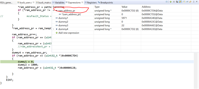
    1.The content of ram_address_pr is 0xC702, but my checking is " if (ram_address_pr == (uint32_t *)0x0000C7D4)". Why the program enters to if loop

    Please find below is disassembly. Note : Breakpoint is @ dummy1 = 0; Based on assembly code. Compared value is 0xC7D4 and the content of "ram_address_pr" is 0xC7D2.

    083537:   6003        SB           $C$L81, NEQ
    793                 ram_address_pr = (uint32_t *)0x0000A000;
    083538:   8F40A000    MOVL         XAR5, #0x00a000
    797             if (ram_address_pr == (uint32_t *)0x0000C7D4)
            $C$L81:
    08353a:   8F00C7D4    MOVL         XAR4, #0x00c7d4
    796             dummy4 = ram_address_pr;
    08353c:   A0AB        MOVL         @P, XAR5
    797             if (ram_address_pr == (uint32_t *)0x0000C7D4)
    08353d:   A8A9        MOVL         @ACC, XAR4
    08353e:   0FAB        CMPL         ACC, @P
    08353f:   600C        SB           $C$L82, NEQ
    800                 dummy2 = 1000;
    083540:   8F0003E8    MOVL         XAR4, #0x0003e8
    083542:   761F028C    MOVW         DP, #0x28c
    799                 dummy1 = 0;
    083544:   0200        MOVB         ACC, #0
    801                 ram_address_pr = (uint32_t *)0x00000128;
    083545:   8F400128    MOVL         XAR5, #0x000128
    083547:   A83C        MOVL         @0x3c, XAR4
    083548:   761F028D    MOVW         DP, #0x28d
    799                 dummy1 = 0;
    08354a:   1E0E        MOVL         @0xe, ACC
    768         for (dummy2 = 0; dummy2 < 597; dummy2++)
            $C$L82:
    08354b:   0201        MOVB         ACC, #1
    08354c:   761F028C    MOVW         DP, #0x28c
    08354e:   073C        ADDL         ACC, @0x3c
    08354f:   1EA7        MOVL         @XAR7, ACC
    083550:   8F000255    MOVL         XAR4, #0x000255
    083552:   1E3C        MOVL         @0x3c, ACC
    083553:   A8A9        MOVL         @ACC, XAR4
    083554:   0FA7        CMPL         ACC, @XAR7
    083555:   66C1        SB           $C$L79, HI
    083556:   A93E        MOVL         @0x3e, P
    083557:   761F031F    MOVW         DP, #0x31f
    083559:   A016        MOVL         @0x16, XAR5
    08355a:   2910        CLRC         INTM
    08355b:   FF69        SPM          #0
    08355c:   0006        LRETR        
            FSK_CORR_DETECTOR_RUN():
    08355d:   E20304BD    MOV32        *SP++, R4H
    08355f:   E20305BD    MOV32        *SP++, R5H
    083561:   E20306BD    MOV32        *SP++, R6H
    083563:   E20307BD    MOV32        *SP++, R7H
    083565:   761F02AC    MOVW         DP, #0x2ac
    083567:   0622        MOVL         ACC, @0x22
    083568:   071E        ADDL         ACC, @0x1e
    083569:   18A87FFF    AND          @AH, #0x7fff
    08356b:   1E22        MOVL         @0x22, ACC
    08356c:   0624        MOVL         ACC, @0x24

    2. As I mentioned, total number blocks of ROM is 5970 by my calculation. I am using 2 variable dummy1 and dummy3 to monitor value of total number block of RAM checked and executed number of the function for 5970 blocks. It is supposed dummy1 and dummy 3 should be 5970 and 10 separately. However, it is 5971 and 11. I cannot find that problem.

    Please find below is a part of MEMORY section in link file

    MEMORY
    {
       BEGIN               : origin = 0x080000, length = 0x000002
       BOOT_RSVD        : origin = 0x00000002, length = 0x00000126
       RAMM0               : origin = 0x00000128, length = 0x000002D8
       RAMM1            : origin = 0x00000400, length = 0x000003F8     /* on-chip RAM block M1 */
    // RAMM1_RSVD       : origin = 0x000007F8, length = 0x00000008 /* Reserve and do not use for code as per the errata advisory "Memory: Prefetching Beyond Valid Memory" */

    /* RAMLS4           : origin = 0x0000A000, length = 0x00000800
       RAMLS5           : origin = 0x0000A800, length = 0x00000800
       RAMLS6           : origin = 0x0000B000, length = 0x00000800
       RAMLS7           : origin = 0x0000B800, length = 0x00000800*/

       /* Combining all the LS RAMs */
       RAMLS4567        : origin = 0x0000A000, length = 0x00002000
       //RAMGS0           : origin = 0x0000C000, length = 0x000007F8
       RAMGS0           : origin = 0x0000C000, length = 0x000007D4
       RAMGS0_TEMPCOPY  : origin = 0x0000C7D4, length = 0x00000024

    where RAMGS0_TEMPCOPY is reserved for my own usage. It will not check.

  • Do you have optimization turned on in the compiler?

    So the comparison in question seems to be "CMPL   ACC, @P", correct? If you step through the code and instead of looking at the Expressions window, look at XAR4, XAR5, ACC, and P (under Core Registers in the CCS Registers view) do the values look okay? In the Dissassembly I can't see where XAR5 previously gets updated, but I'm wondering if it's different from what the Expressions window is showing for ram_address_pr.

    Whitney

  • Hi Whitney

    1. Yes, optimization is turn on with option 4 and speed vs size trade-offs is 5

    2. I am not familiar with assemble very well and hence not understand your meaning. Sorry. Could you explain more?

    3. I view the content of these registers ACC=0xC7D4, P=0xC7D4, XAR4=0x03E8 and XAR5=0xC7D4.  I make a breakpoint @ code "dummy1 = 0" during view the content of register with optimization level 4.

    4. I do some test. I configure optimization level to 0. CCS expression view shows a correct value of the pointer.

    Based on finding on #3 and #4, could I say that the problem is related to CCS compiler display problem only? No impact on functional of firmware.

    Furthermore, I still don't identify the problem on number of execution of the function.

    BR

    HK Woo

  • The Expressions window is specifically looking at where ram_address_pr is stored in RAM, so what it isn't showing you is that the code has optimized away some accesses to that RAM location and is instead using XAR5 to hold the current address being checked. By looking at the Core Registers and the disassembly, I can tell that XAR5 = ACC = ram_address_pr = 0xC7D4 and P = 0xC7D4 and therefore the instruction that checks if P == ACC results in the if statement executing.

    The actual variable in memory doesn't get updated until quite a few instructions later (looks like the instruction at 0x083559 in what's shown above). It seems to me that the code is doing the right thing, but the high level of optimization is obscuring it from a Expressions window perspective.

    Whitney

  • Whitney

    Thanks for your update. How about the number of function execution. It is expected that it is 5970 times to complete the RAM section. Please find below information of section in link find

    MEMORY
    {
       BEGIN               : origin = 0x080000, length = 0x000002
       BOOT_RSVD        : origin = 0x00000002, length = 0x00000126
       RAMM0               : origin = 0x00000128, length = 0x000002D8
       RAMM1            : origin = 0x00000400, length = 0x000003F8     /* on-chip RAM block M1 */
    // RAMM1_RSVD       : origin = 0x000007F8, length = 0x00000008 /* Reserve and do not use for code as per the errata advisory "Memory: Prefetching Beyond Valid Memory" */

    /* RAMLS4           : origin = 0x0000A000, length = 0x00000800
       RAMLS5           : origin = 0x0000A800, length = 0x00000800
       RAMLS6           : origin = 0x0000B000, length = 0x00000800
       RAMLS7           : origin = 0x0000B800, length = 0x00000800*/

       /* Combining all the LS RAMs */
       RAMLS4567        : origin = 0x0000A000, length = 0x00002000
       //RAMGS0           : origin = 0x0000C000, length = 0x000007F8
       RAMGS0           : origin = 0x0000C000, length = 0x000007D4
       RAMGS0_TEMPCOPY  : origin = 0x0000C7D4, length = 0x00000024
    // RAMGS0_RSVD      : origin = 0x0000C7F8, length = 0x00000008 /* Reserve and do not use for code as per the errata advisory "Memory: Prefetching Beyond Valid Memory" */

  • Are you going one too far in RAMM1? The length of M1 is 0x3F8 but you're stopping when the address is 0x7FA, but for the end of GS0, the length is 0x7D4 and you're stopping at 0xC7D4.

    Whitney

  • Whitney

    Thanks for your finding. The issue is fixed. I think that IEC 60730 ram testing should be ok. However, I still have a question TI STL_CPU_REG_checkCPURegisters(). Should you share a pseudo -code for the function to me so that I can demonstrate to safety agency during co-test with them.

    BR

    HK WOo

  • See if the attached it helpful. I saved it as a .c file for the syntax highlighting  in my text editor, but it is obviously not executable C code.

    1
    2
    3
    4
    5
    6
    7
    8
    9
    10
    11
    12
    13
    14
    15
    16
    17
    18
    19
    //
    // To keep pseudo code less complicated, adjustment of the length of the
    // pattern given the size of the register is not shown below. REG_TEST_PATTERN
    // will either mean 0xAAAA or 0xAAAAAAAA depending on what is appropriate for
    // the register being tested.
    //
    REG_TEST_PATTERN = 0xAAAA or 0xAAAAAAAA
    REG_ERROR_PATTERN = 0x555D
    ST1_CLR_TEST_MASK = 0xFF5B // PAGE0 is always 1, IDLESTAT and LOOP not tested
    ST1_SET_TEST_MASK = 0x0A00 // M0M1MAP and OBJMODE are always 1
    TEST_ITERATIONS = 1
    uint16_t STL_CPU_REG_testCPURegisters(bool injectError)
    {
    [context save (see conventions in https://www.ti.com/lit/pdf/spru514)]
    //************************************************************************
    XXXXXXXXXXXXXXXXXXXXXXXXXXXXXXXXXXXXXXXXXXXXXXXXXX

    Whitney

  • Hi Whitney

    I showed the pseudo-code to safety agency, they said that they are reviewing it. Besides of it, they asked an question, how to test the function. I told them, we can includes the parameter true in the function to generate an error, but they said that it is not a good idea, they want to change the value of register manually during the testing in debug mode. Could you advice how to do it?

    HK Woo

  • Yes, in debug mode you can definitely do that. The CPU registers are available under "Core Registers" in the CCS Registers window. For any of the registers you can put a breakpoint at the line after the test pattern is written to the register but before the comparison is done, flip a bit in that register in the Registers window and then run the application to make sure it returns a failure.

    For example, below I put a breakpoint on line 51 after MOVL XT, @ACC (move the pattern, which is stored in the ACC register, into the XT register) and flipped a bit in the XT register in the registers window (changed 0x55555555 to 0x55555545). Then when I single stepped through it, I could see it take that branch to failCPURegTest where the return value was set to indicate a failure.

    Whitney