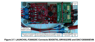
Other Parts Discussed in Thread: BOOSTXL-DRV8323RS, LAUNCHXL-F280025C, DRV8323
When going through the Universal Motor Control Project and Lab User's Guide section 2.2.5 (BOOSTXL-DRV8323RS Setup) it describes a few modifications which I'm hoping someone can provide an explanation for:
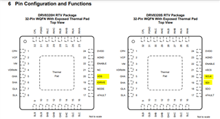
1. Why are pins J3-29, J3-30 of F280025C disconnected from BOOSTXL-DRV8323RS?
2. Why are pins J4-4 and J4-18 connected using a jumper wire? What is the purpose of connecting, as per the guide, DRV_SCS and SPI_STE?
And a follow up question, if I'd like to connect a second BOOSTXL-DRV8323RS to my LAUNCHXL-F280025C (using connector site 2), do I have to repeat these modifications?
Regards,