This thread has been locked.
If you have a related question, please click the "Ask a related question" button in the top right corner. The newly created question will be automatically linked to this question.
BACKGROUND: Trying to insert a look up table FUNCTION for three pulses that are coming from external hardware to three GPIOs using OUTPUT LUT BLOCK: CLB MODULE, and the output needs to be used in ECAP. So, I need to see the output signal from OUTPUT LUT BLOCK to a GPIO initially to see its nature using OSCILLOSCOPE and then connect to ECAP1. Got confused in many places while going through "spruin7a".
1. I am using following codes:
CLB INPUT X-BAR is used as input of three GPIOs as following:
ClbInputXbarRegs.INPUT1SELECT= 11; // GPIO11 AS CLB INPUT
ClbInputXbarRegs.INPUT1SELECT= 27; // GPIO27 AS CLB INPUT
ClbInputXbarRegs.INPUT1SELECT= 42; // GPIO42 AS CLB INPUT
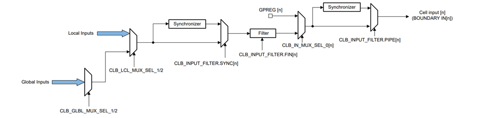
so that CLB INPUT X-BAR signal can go to the input of OUTPUT LUT BLOCK: CLB MODULE in page number 1279, Figure 12-14.
2. Page 1271, Table 12-4 defines 8 "external signals" 23 to 31 as INPUT to OUTPUT LUT BLOCK: CLB MODULE. However, confused on: which signals constitute these external signals ?
3. How these 8 numbers of "external signals" are connected to INPUT1-INPUT16 signals coming out of CLB INPUT X-BAR in page 1265, Figure 12-5.
4. Let me know which are the associated registers I need to configure for my purpose ?
Sibarasad,
I think there is a HUGE piece missing here.
I feel like:
1. You are using bitfields - You should be using driverlib
2. You are not using the CLB TOOL - GUI tool.
3. You are not using C2000 SysConfig - (it has an integrated CLB TOOL)
4. You havent found the CLB examples that showcase all of these connections.
You would need to go through these material and then everything will make so much sense.
Would you like to see the resources for the items above?
what type of support it is ??? I am very specific to all of my questions mentioning pages and tables.
Can you be particular and very specific in your answer in all 4 questions ? If you do NOT have time pass on to somebody else.
"I think there is a HUGE piece missing here." what piece s missing, refer to document i need to go through.
SIBAPRASAD, (not sibarasad ?? at least be correct on my name !!!)
SIBAPRASAD,
I think what is happening is that you are trying to HAND CODE the CLB which will take alot of time from your side. I am trying to save you time.
Here is the answer to your questions:
1. CLB Input XBAR selections are available at the local mux:
You then have to select the local mux input you want to route it to a BOUNDARY INx. Then route the BOUNDARY inx (now you are in the tile) to OUTLUT in the actual tile,
2. External inputs to the TILE are the BOUNDARY INx signals. In the CLB GUI tool they are available as a drop down.
3. These 8 BOUNDARY INx signals are comming from various muxes.
4. Again, the resigters you are trying to configure/code for configuring them would all be generated for you by the GUI tool. But if you want to configure them manually you have to configure:
Thanks Nima, Great explaining,
Comment: I am NOT sure how the GUI tool is going to help people !! A person still needs to understand the signal routing and registers involved for manipulation. The code generated from GUI appears to me as a black box and very difficult to manipulate. You can get a second opinion from a person who has a POWER background. People I know hold the same opinion.
However, thanks for taking time to explain: the documentation should have used "BOUNDARY INx" in place of "External Inputs" and that could have make my life easier.
I will get back after implementing,
Regards,
SIBAPRASAD
SIBAPRASAD,
I think the GUI tool can help guide in writing your code. I agree that the user still has to understand the connections.
I would recommend looking at example 8 in the CLB folder of the C2000Ware's latest release.
There are also examples for CLB INPUT XBAR, CLB OUTPUT XBAR and others.
For the CLB specifically you are better off using the tool.
For example on a LUT3 (OUTPUT LUT) you have 3 inputs, i0, i1, i2 and an OUT.
Let's say you want to implement: (i0&i1)|i2^i0
What would be the register value for this logic? and every time you change it you would have to figure out the register value.
In the GUI tool, you literally just type: (i0&i1)|i2^i0
It is really powerful.
You know we had the CLB in our devices for 3 years and we didn't expose it to customers until we had the SysConfig GUI tool because we knew it would be difficult to configure.
From someone that has worked with the CLB for 6 years, I promise, you would benefit from switching to the GUI tools.
Thanks NIMA,
I respect your opinion, however disagree with you on this GUI tool to develop code. You need to take a holistic view, NOT just code development as an isolated task. See, code is developed for a target POWER HARDWARE, we have headache to make POWER HARDWARE functional to desired performance. So, a POWER guy needs to comprehend complete process from POWER HARDWARE ckts, uC board ckts and FIRMWARE code. So, each process needs to be very very transparent and understandable. Keeping that in mind, CLB TOOL needs to be very very transparent and comprehensive. Ultimately, few registers needs to be configured to get desired logic to be implemented and the CODER needs to have deep understanding on exactly which registers he is configuring and why. I would argue that you need to have better block diagram on CLB describing connectivity between various elements. Nobody wants to develop code quickly, however wants to develop code that is comprehended and manipulated easily.
Contrary, GUI is a black box, generates code that might not be understandable to people and ultimately adds to more stress to the programmer. I guess, this is a good tool for beginners who wants to play with the uC, NOT for POWER expert who wants to make POWER hardware working with uC. You might be aware, people have difficulty in engaging a POWER guy and a CODER to make system working because they do NOT understand each other. This problem is known for long.
This TMS320F280023 processor is way way better than piccolo and I am in love with it. However, sometimes I feel that TI is in a hurry to document it. I will expect more extensive documentation on CLB. Please make good block diagrams as you people did for PWM, GPIO etc, that will help. Sorry for contradicting,
Regards
Dr. SIBAPRASAD CHAKRABARTI, PhD,
Power Electronics, University of Wisconsin-Madison, USA
BACKGROUND: I have three pulses (120 deg apart in time domain having 333Hz frequency each) from external hardware as input to three GPIOs: 11, 27 and 42 and the following code works as when these GPIO signals guided to XBAR and then routed to three eCAPs and I am able to calculate the period of these pulses and display period values in my watch window successfully. I am using TI LAUNCHXL-F280025C board for this experiment.
/////////////////////////////////////////////////////////////////////////////////////////////////////
EALLOW;
InputXbarRegs.INPUT1SELECT = 11; //11, page 798 figure
InputXbarRegs.INPUT2SELECT = 27; //27
InputXbarRegs.INPUT3SELECT = 42; //42
EDIS;
ECap1Regs.ECCTL0.bit.INPUTSEL=0; // page 1986
ECap2Regs.ECCTL0.bit.INPUTSEL=1;
ECap3Regs.ECCTL0.bit.INPUTSEL=2;
/////////////////////////////////////////////////////////////////////////////////////////////////////
Now, I want to XOR these three GPIO pulses and the XORed signal as input to eCAP1 only. Please see my following code and let me know which other registers I need to configure since I am NOT getting the period value of the XORed signal in eCAP1 in the watch window ??????
/////////////////////////////////////////////////////////////////////////////////////////////////////
CpuSysRegs.PCLKCR17.bit.CLB1=1; // enable CLB1 clock
EALLOW;
ClbInputXbarRegs.INPUT1SELECT= 11; // GPIO11 as CLB INPUT X-BAR INPUT, page 1265, Table 12-5
ClbInputXbarRegs.INPUT2SELECT= 27; // GPIO27 as CLB INPUT X-BAR INPUT
ClbInputXbarRegs.INPUT3SELECT= 42; // GPIO42 as CLB INPUT X-BAR INPUT
// INPUT1 from CLB INPUT X-BAR is configured as Local signal and passed as BOUNDARY IN_0 (inside CLB tile already), page 1256, Fig. 12-4, Table 12-2
Clb1LogicCtrlRegs.CLB_LCL_MUX_SEL_1.bit.LCL_MUX_SEL_IN_0=48;
Clb1LogicCtrlRegs.CLB_LCL_MUX_SEL_1.bit.LCL_MUX_SEL_IN_1=49;
Clb1LogicCtrlRegs.CLB_LCL_MUX_SEL_1.bit.LCL_MUX_SEL_IN_3=50;
// External Input 0 (BOUNDARY IN_0) as IN_0 to OUTPUT LUT block of CLB through STATIC SWITCH BLOCK, page 1271, Table 12-4, page 1279, Fig. 12-14
Clb1LogicCfgRegs.CLB_OUTPUT_LUT_7.bit.IN0=24;
Clb1LogicCfgRegs.CLB_OUTPUT_LUT_7.bit.IN1=25;
Clb1LogicCfgRegs.CLB_OUTPUT_LUT_7.bit.IN2=26;
Clb1LogicCfgRegs.CLB_OUTPUT_LUT_7.bit.FN=0x96; // XOR function LUT
Clb1LogicCtrlRegs.CLB_OUT_EN=0xFFFF;
Clb1LogicCfgRegs.CLB_MISC_ACCESS_CTRL.bit.BLKEN=1;// allow CLB1_OUTx to CLB OUTPUT X-BAR, page 1267, Fig. 12-7, Reg: page 1340, Table: 12-57
do i need this above line, if yes what for ?
// ClbOutputXbarRegs.OUTPUT1MUX0TO15CFG.bit.MUX0=0; // CLB1_OUT0 to CLB_OUTPUT_XBAR_1 output signal, page 806, Table 9-6
EDIS;
ECap1Regs.ECCTL0.bit.INPUTSEL=17; //eCAP input from CLB1_CLBOUT15 (which is CLB1_CLBOUT7, page 1266, Table 12-6) page 1960, Table 18-1
///////////////////////////////////////////////////////////////////////////////////////////////////////////
Clb1LogicCtrlRegs.CLB_OUT_EN=0xFFFF;
Why are you setting the CLB_OUT_EN to 0xFFFF ?
This will cause the CLB OUTPUTs to override all kinds of signals internal to the device.
You only really need to set it for BIT15 to get the ECAP signal enabled.
ECap1Regs.ECCTL0.bit.INPUTSEL=17;
This is correct.
Can you tell me the final value in your CFG OUTLUT7 register?
This is what I get from the CLB tool:
Thanks NIMA,
Q1. I got CLB_OUTPUT_LUT_7=0x004B6B38 as yours, but what's the second value 556B38 in your reply ?
Q2. Even if 0x004B6B38 matches with yours, I am NOT getting period value of eCAP !!
Q3. Do I need any other register configure ???
1. The second value in red is the old value. The tool shows you a live change log as you change the settings in the tool. The green one is the important one and it matches.
Q3. I think the only other thing that could be causing the probelm is the mux select signals. I think the boundary in configuration for all of the muxes may be incorrect. Before we look into that, if you bring out the signal for OUTLUT7 to a GPIO using OUTPUTXBAR, can you see the XORed signal?
Thanks NIMA for your continued support,
Q1. See, I was getting period values of eCAP1, eCAP2, eCAP3 in watch window in my previous program using INPUTXBAR.
Q2. I used the same GPIO signals in the later program, however used CLB INPUT XBAR and OUTPUT LUT, so MUX selection i used is:
EALLOW;
ClbInputXbarRegs.INPUT1SELECT= 11; // GPIO11 as CLB INPUT X-BAR INPUT, page 1265, Table 12-5
ClbInputXbarRegs.INPUT2SELECT= 27; // GPIO27 as CLB INPUT X-BAR INPUT
ClbInputXbarRegs.INPUT3SELECT= 42; // GPIO42 as CLB INPUT X-BAR INPUT
Clb1LogicCtrlRegs.CLB_LCL_MUX_SEL_1.bit.LCL_MUX_SEL_IN_0=48;
Clb1LogicCtrlRegs.CLB_LCL_MUX_SEL_1.bit.LCL_MUX_SEL_IN_1=49;
Clb1LogicCtrlRegs.CLB_LCL_MUX_SEL_1.bit.LCL_MUX_SEL_IN_3=50;
EDIS;
Q3. Can you send me the all register values of CLB1 peripheral.
do i need to configure ? SysPeriphAcRegs.CLB1_AC.bit.CPU1_ACC=3;
Here is the CLB1 register values, I can see some registers have non zero values. Please check any discrepancy,
SysPeriphAcRegs.CLB1_AC.bit.CPU1_ACC=3;
These are the access control registers. I don't this is affecting it.
Let me get a set of functions that would have to get set to take your signals into the CLB.
Nima
Okay so here is what I have:
1. CLB Input XBAR setting:
2. CLB Mux selection (local mux, select the CLB INPUT XBAR entries):
3. The CLB tile configuration
Then finally, follow by overriding the ECAP signals.
This would be all that is needed.
Thanks NIMA,
Looks like these are all abut configuration, is the code loaded into a processor and validated ?
All of the generated code has been validated at design time. If you load the code into your device, you can check to see what the register values are and compare them with your manual code.
The items that you want to check is to see if the CLB_configLocalInputMux and CLB_configGlobalInputMux modify the registers as you did. There are sometimes some additional bits that get set to ensure the configuration is correct, for example:
You have to have line 71 for line 70 to propagate through the muxes.
Thanks NIMA for your continuing support,
Can you send me the CLB1 register values after they are configured, I will cross check.
I am also facing problem in adding SYSTEM CONFIG in my existing project and things get going.., I will post the problem...
I went ahead and grabbed the values for you. I am not supposed to really run the code but I want you to be able to check this as fast as possible.
Clb1LogicCfgRegs Register Group CLB_COUNT_RESET Register 0x00000000 CLB_COUNT_MODE_1 Register 0x00000000 CLB_COUNT_MODE_0 Register 0x00000000 CLB_COUNT_EVENT Register 0x00000000 CLB_FSM_EXTRA_IN0 Register 0x00000000 CLB_FSM_EXTERNAL_IN0 Register 0x00000000 CLB_FSM_EXTERNAL_IN1 Register 0x00000000 CLB_FSM_EXTRA_IN1 Register 0x00000000 CLB_LUT4_IN0 Register 0x00000000 CLB_LUT4_IN1 Register 0x00000000 CLB_LUT4_IN2 Register 0x00000000 CLB_LUT4_IN3 Register 0x00000000 CLB_FSM_LUT_FN1_0 Register 0x00000000 CLB_FSM_LUT_FN2 Register 0x00000000 CLB_LUT4_FN1_0 Register 0x00000000 CLB_LUT4_FN2 Register 0x00000000 CLB_FSM_NEXT_STATE_0 Register 0x00000000 CLB_FSM_NEXT_STATE_1 Register 0x00000000 CLB_FSM_NEXT_STATE_2 Register 0x00000000 CLB_MISC_CONTROL Register 0x00000000 CLB_OUTPUT_LUT_0 Register 0x00000000 CLB_OUTPUT_LUT_1 Register 0x00000000 CLB_OUTPUT_LUT_2 Register 0x00000000 CLB_OUTPUT_LUT_3 Register 0x00000000 CLB_OUTPUT_LUT_4 Register 0x00000000 CLB_OUTPUT_LUT_5 Register 0x00000000 CLB_OUTPUT_LUT_6 Register 0x00000000 CLB_OUTPUT_LUT_7 Register 0x004B6B38 CLB_HLC_EVENT_SEL Register 0x00000000 CLB_COUNT_MATCH_TAP_SEL Register 0x00000000 CLB_OUTPUT_COND_CTRL_0 Register 0x00000000 CLB_OUTPUT_COND_CTRL_1 Register 0x00000000 CLB_OUTPUT_COND_CTRL_2 Register 0x00000000 CLB_OUTPUT_COND_CTRL_3 Register 0x00000000 CLB_OUTPUT_COND_CTRL_4 Register 0x00000000 CLB_OUTPUT_COND_CTRL_5 Register 0x00000000 CLB_OUTPUT_COND_CTRL_6 Register 0x00000000 CLB_OUTPUT_COND_CTRL_7 Register 0x00000000 CLB_MISC_ACCESS_CTRL Register 0x0000 CLB_SPI_DATA_CTRL_HI Register 0x0000
Clb1LogicCtrlRegs Register Group CLB_LOAD_EN Register 0x0002 CLB_LOAD_ADDR Register 0x0000003F CLB_LOAD_DATA Register 0x00000800 CLB_INPUT_FILTER Register 0x00000000 CLB_IN_MUX_SEL_0 Register 0x00000000 CLB_LCL_MUX_SEL_1 Register 0x70004A30 CLB_LCL_MUX_SEL_2 Register 0x00000000 CLB_BUF_PTR Register 0x00000000 CLB_GP_REG Register 0x00000000 CLB_OUT_EN Register 0x00020000 CLB_GLBL_MUX_SEL_1 Register 0x00000000 CLB_GLBL_MUX_SEL_2 Register 0x00000000 CLB_PRESCALE_CTRL Register 0x00000000 CLB_INTR_TAG_REG Register 0x0000 CLB_LOCK Register 0x00000000 CLB_HLC_INSTR_READ_PTR Register 0x0000 CLB_HLC_INSTR_VALUE Register 0x0800 CLB_DBG_OUT_2 Register 0x00000780 CLB_DBG_R0 Register 0x00000000 CLB_DBG_R1 Register 0x00000000 CLB_DBG_R2 Register 0x00000000 CLB_DBG_R3 Register 0x00000000 CLB_DBG_C0 Register 0x00000000 CLB_DBG_C1 Register 0x00000000 CLB_DBG_C2 Register 0x00000000 CLB_DBG_OUT Register 0x800F0F0E
Nima