This thread has been locked.

If you have a related question, please click the "Ask a related question" button in the top right corner. The newly created question will be automatically linked to this question.

TMDSPREX28335: Improper data logging and viewing in the GRAPH window while reading information from ADC

Part Number: TMDSPREX28335
Other Parts Discussed in Thread: C2000WARE, CONTROLSUITE

Hi Team,

I'm posting on behalf of the customer.

I am using a TMDSPREX28335 board. I am trying to dump an external sinusoidal signal (grid voltage which is 50 Hz) into the controller using its ADC port. The signal is well conditioned and is between the safety limits of 0 and 3 Volts.

Initially, I had tied the ADC to CPU Timer0 Interrupt (happening every 25 micro seconds or 40 kHz) and observed the signal in the GRAPH window.

The code for ADC triggered by CPU TIMER0 Interrupt is as follows:

#include "math.h"

#include "IQmathlib.h"

#include "DSP2833x_Device.h"     // DSP2833x Headerfile Include File

#include "DSP2833x_Examples.h"   // DSP2833x Examples Include File


// Prototype statements for functions found within this file.

interrupt void cpu_timer0_isr(void);


// Variables used for plotting, reading from ADC and interrupt count

Uint32 count=1;

int sample = 0;

float array_sine[800];

float voltage_grid = 0, vg1 = 0, voltage_offset = 0, voft1 = 0;


main()

{

    InitSysCtrl();

//    EALLOW;

//    SysCtrlRegs.HISPCP.all = 0x3;  // HSPCLK = SYSCLKOUT/6

//    EDIS;

    DINT;   // disable CPU interrupts

    InitPieCtrl();  // disable all peripheral interrupts

    EALLOW;

    SysCtrlRegs.PCLKCR0.bit.TBCLKSYNC = 0;      // Stop all the TB clocks

    EDIS;

    EALLOW;

    SysCtrlRegs.PCLKCR0.bit.TBCLKSYNC = 1;         // Start all the timers synced

    EDIS;

    IER = 0x0000;   // disables all interrupts

    IFR = 0x0000;   // clears flags of all interrupts

    InitPieVectTable();


//************ADC INITIALISATION and CONFIGURATION BEGINS************//

    InitAdc();                               // basic ADC setup (including calibration)

    AdcRegs.ADCTRL1.all = 0;                 // clear ADCTRL1 before initializing

    AdcRegs.ADCTRL1.bit.ACQ_PS = 0xf;        // sample and hold for (15+1)=16 ADC cycles

    AdcRegs.ADCTRL1.bit.CPS = 0;             // divide further by 1

    AdcRegs.ADCTRL1.bit.SEQ_CASC = 1;        // cascaded mode for ADC (16 states)

    AdcRegs.ADCTRL1.bit.CONT_RUN = 0;        // continuous run mode for ADC disabled


//    AdcRegs.ADCTRL2.all = 0;                 // clear ADCTRL2 before initializing

    AdcRegs.ADCTRL2.bit.INT_ENA_SEQ1 = 1;      // enable interrupt on SEQ1

    AdcRegs.ADCTRL2.bit.INT_MOD_SEQ1 = 0;    // enable interrupt every end of sequence

    AdcRegs.ADCTRL2.bit.RST_SEQ1 = 1;        // reset SEQ1

    AdcRegs.ADCTRL2.bit.SOC_SEQ1 = 0;        // start SEQ1 from ePWM1_SOCA trigger


    AdcRegs.ADCTRL3.bit.SMODE_SEL = 0;       // sequential simultaneous conversion for ADC

    AdcRegs.ADCTRL3.bit.ADCCLKPS = 3;        // 3 because HSPCLK for ADC is 75 Mhz (150/6); see above

                                                 // from DSP2833x_SysCtrl.c FCLK for ADC is 75 MHz and not 150 MHz;

                                                 // 75/(2*3) = 12.5 MHz


    AdcRegs.ADCMAXCONV.all = 0x0001;              // 2 conversions

    AdcRegs.ADCCHSELSEQ1.bit.CONV00 = 0x2;     // assign ADCINA2 to conv00

    AdcRegs.ADCCHSELSEQ1.bit.CONV01 = 0x3;     // assign ADCINA3 to conv01


//************ADC INITIALISATION and CONFIGURATION ENDS************//


    EALLOW;  // This is needed to write to EALLOW protected registers

    PieVectTable.TINT0 = &cpu_timer0_isr;

    EDIS;


    InitCpuTimers();

    ConfigCpuTimer(&CpuTimer0, 150, 25); // generate TINT0 at 25 us or 40 kHz

    CpuTimer0Regs.TCR.all = 0x4001;       // disable cpu timer0 interrupt (not needed)


   IER |= 1; // Enable all of INT1 group

   PieCtrlRegs.PIEIER1.bit.INTx7 = 1;   // enable ADC INT (6th interrupt in group 1)

   EINT;          // Enable Global interrupt INTM

   ERTM;          // Enable Global realtime interrupt DBGM


}


interrupt void cpu_timer0_isr(void)

{

    count++;                                    // check if interrupt is being generated

    AdcRegs.ADCTRL2.bit.SOC_SEQ1 = 1;

    voltage_grid = AdcRegs.ADCRESULT0>>4;       // read from ADC

    voltage_offset = AdcRegs.ADCRESULT1>>4;     // read from ADC

    vg1 = voltage_grid*3/4095;                  // get original value

    voft1 = voltage_offset*3/4095;              // get original value


        if (sample > 799)

            sample = 0;

        array_sine[sample] = vg1;

        sample++;


  // Reinitialize for next ADC sequence

  AdcRegs.ADCTRL2.bit.RST_SEQ1 = 1;         // Reset SEQ1

  AdcRegs.ADCST.bit.INT_SEQ1_CLR = 1;       // Clear INT SEQ1 bit

  PieCtrlRegs.PIEACK.all = PIEACK_GROUP1;   // Acknowledge interrupt to PIE

}


//===========================================================================

// End of SourceCode.

//===========================================================================

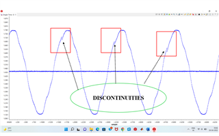
The graph corresponding to the above code is this:

As you can see there is a discontinuity in the (converted) viewed signal.

I then reattempted by giving command to the ADC from the ePWM1 Interrupt (under the same conditions i.e., every 25 micro seconds or 40 kHz). The code for ADCSoC from ePWM1 Interrupt is as follows:

/*      OBJECTIVE:

 * a) use ePWM1 triggered ADC interrupt at 25 us

 * b) ADC in cascaded mode

 * c) ADC does sequential sampling

 * d) ACQ_PS = 0xf (15+1=16 hold cycles)

 * e) ADC frequency is 12.5 MHz

 * f) observe the plot

 */


#include "math.h"

#include "IQmathlib.h"

#include "DSP2833x_Device.h"     // DSP2833x Headerfile Include File

#include "DSP2833x_Examples.h"   // DSP2833x Examples Include File


// Prototype statements for functions found within this file.

void InitEPwmTimer(void);

interrupt void adc_isr(void);


// Variables used for plotting, reading from ADC and interrupt count

Uint32 count=1;

int sample = 0;

float array_sine[800];

float voltage_grid = 0, vg1 = 0, voltage_offset = 0, voft1 = 0;


main()

{

    InitSysCtrl();

//    EALLOW;

//    SysCtrlRegs.HISPCP.all = 0x3;  // HSPCLK = SYSCLKOUT/6

//    EDIS;

    DINT;   // disable CPU interrupts

    InitPieCtrl();  // disable all peripheral interrupts

    EALLOW;

    SysCtrlRegs.PCLKCR0.bit.TBCLKSYNC = 0;      // Stop all the TB clocks

    EDIS;

    InitEPwmTimer();    // initiate the required ePWM registers and configure interrupt requirements

    EALLOW;

    SysCtrlRegs.PCLKCR0.bit.TBCLKSYNC = 1;         // Start all the timers synced

    EDIS;

    IER = 0x0000;   // disables all interrupts

    IFR = 0x0000;   // clears flags of all interrupts

    InitPieVectTable();


//************ADC INITIALISATION and CONFIGURATION BEGINS************//

    InitAdc();                               // basic ADC setup (including calibration)

    AdcRegs.ADCTRL1.all = 0;                 // clear ADCTRL1 before initializing

    AdcRegs.ADCTRL1.bit.ACQ_PS = 0xf;        // sample and hold for (15+1)=16 ADC cycles

    AdcRegs.ADCTRL1.bit.CPS = 0;             // divide further by 1

    AdcRegs.ADCTRL1.bit.SEQ_CASC = 1;        // cascaded mode for ADC (16 states)

    AdcRegs.ADCTRL1.bit.CONT_RUN = 0;        // continuous run mode for ADC disabled


//    AdcRegs.ADCTRL2.all = 0;                 // clear ADCTRL2 before initializing

    AdcRegs.ADCTRL2.bit.INT_ENA_SEQ1 = 1;      // enable interrupt on SEQ1

    AdcRegs.ADCTRL2.bit.INT_MOD_SEQ1 = 0;    // enable interrupt every end of sequence

    AdcRegs.ADCTRL2.bit.RST_SEQ1 = 1;        // reset SEQ1

    AdcRegs.ADCTRL2.bit.EPWM_SOCA_SEQ1 = 1;        // start SEQ1 from ePWM1_SOCA trigger


    AdcRegs.ADCTRL3.bit.SMODE_SEL = 0;       // sequential simultaneous conversion for ADC

    AdcRegs.ADCTRL3.bit.ADCCLKPS = 3;        // 3 because HSPCLK for ADC is 75 Mhz (150/6); see above

                                                 // from DSP2833x_SysCtrl.c FCLK for ADC is 75 MHz and not 150 MHz;

                                                 // 75/(2*3) = 12.5 MHz


    AdcRegs.ADCMAXCONV.all = 0x0001;              // 2 conversions

    AdcRegs.ADCCHSELSEQ1.bit.CONV00 = 0x2;     // assign ADCINA2 to conv00

    AdcRegs.ADCCHSELSEQ1.bit.CONV01 = 0x3;     // assign ADCINA3 to conv01


//************ADC INITIALISATION and CONFIGURATION ENDS************//


    EALLOW;  // This is needed to write to EALLOW protected registers

    PieVectTable.ADCINT = &adc_isr;

    EDIS;


    InitCpuTimers();

    ConfigCpuTimer(&CpuTimer0, 150, 25); // generate TINT0 at 25 us or 40 kHz

//    CpuTimer0Regs.TCR.all = 0x4001;       // disable cpu timer0 interrupt (not needed)


   IER |= 1; // Enable all of INT1 group

   PieCtrlRegs.PIEIER1.bit.INTx6 = 1;   // enable ADC INT (6th interrupt in group 1)

   EINT;          // Enable Global interrupt INTM

   ERTM;          // Enable Global realtime interrupt DBGM


}


void InitEPwmTimer(void)

{

    EALLOW;

    GpioCtrlRegs.GPAMUX1.bit.GPIO0 = 1; // ePWM1A active

    GpioCtrlRegs.GPAMUX1.bit.GPIO1 = 1; // ePWM1B active

    EDIS;


//      ePWM 1 module clock sync disabled


//      ePWM1 TBCTL INITIALISATIONS

    EPwm1Regs.TBCTL.bit.FREE_SOFT = 11;     // free run

    EPwm1Regs.TBCTL.bit.PHSDIR = 1;         // count up after sync

    EPwm1Regs.TBCTL.bit.CLKDIV = 0;         // TBCLK = HSPCLK/1

    EPwm1Regs.TBCTL.bit.HSPCLKDIV = 1;      // HSPCLK = SYSCLK/2

    EPwm1Regs.TBCTL.bit.SWFSYNC = 0;        // software sync disabled

    EPwm1Regs.TBCTL.bit.SYNCOSEL = 3;       // disable sync

    EPwm1Regs.TBCTL.bit.PRDLD = 0;          // load on CTR = 0

    EPwm1Regs.TBCTL.bit.PHSEN = 0;          // phase enable disabled

    EPwm1Regs.TBCTL.bit.SYNCOSEL = 3;       // disable sync

    EPwm1Regs.TBCTL.bit.CTRMODE = 0;        // count in up-mode


//      ePWM1 ETPS INITIALISATIONS

    EPwm1Regs.ETPS.bit.SOCBCNT = 0;         // this is a read only bit

    EPwm1Regs.ETPS.bit.SOCBPRD = 0;         // disabled because interrupt is to be generated by ePWM1A

    EPwm1Regs.ETPS.bit.SOCACNT = 0;         // this is a read only bit

    EPwm1Regs.ETPS.bit.SOCAPRD = 1;         // interrupt is to be generated by ePWM1A every time

    EPwm1Regs.ETPS.bit.INTCNT = 0;          // read only bit doesn't matter

    EPwm1Regs.ETPS.bit.INTPRD = 1;          // generate interrupt every event


//      ePWM1 ETSEL INITIALISATIONS

    EPwm1Regs.ETSEL.bit.SOCBEN = 0;         // disable SOCB

    EPwm1Regs.ETSEL.bit.SOCBSEL = 0;        // because SOCB is disabled

    EPwm1Regs.ETSEL.bit.SOCAEN = 1;         // enable SOCA

    EPwm1Regs.ETSEL.bit.SOCASEL = 1;        // generate interrupt when CTR = 0

    EPwm1Regs.ETSEL.bit.INTEN = 0;          // disable PWM interrupt

    EPwm1Regs.ETSEL.bit.INTSEL = 0;         // doesn't matter as PWM interrupt is disabled


//      ePWM1 ETSEL INITIALISATIONS

    EPwm1Regs.TBPRD = 1875;                 // fpwm = 40 khz = finterrupt

}


interrupt void adc_isr(void)

{

    count++;                                    // check if interrupt is being generated

    voltage_grid = AdcRegs.ADCRESULT0>>4;       // read from ADC

    voltage_offset = AdcRegs.ADCRESULT1>>4;     // read from ADC

    vg1 = voltage_grid*3/4095;                  // get original value

    voft1 = voltage_offset*3/4095;              // get original value


        if (sample > 799)

            sample = 0;

        array_sine[sample] = vg1;

        sample++;


  // Reinitialize for next ADC sequence

  AdcRegs.ADCTRL2.bit.RST_SEQ1 = 1;         // Reset SEQ1

  AdcRegs.ADCST.bit.INT_SEQ1_CLR = 1;       // Clear INT SEQ1 bit

  PieCtrlRegs.PIEACK.all = PIEACK_GROUP1;   // Acknowledge interrupt to PIE

}


//===========================================================================

// End of SourceCode.

//===========================================================================


And the corresponding output in the graph window is as follows:

As you can see in both the cases (be it ADC connected to TIMER0 interrupt or ADC connected to ePWM1 interrupt) I am getting discontinuous data even though I am collecting 800 points (50 Hz = 20 milli seconds, 40 kHz = 25 us; 20m/25u = 800 points) and plotting all of them.

Another interesting thing is that even though the ADCTRL2 should either show 0x4800 or 0x2800 (depending on RST = 1 or SOC = 1) in case of TIMER0 Interrupt or 0x4900 or 0x0999 (depending on RST = 1 or 0) in case of SOC by ePWM1. However, ACTRL2 is maintaining a permanent value of 0x0800 for TIMER0 and 0x0900 for ePWM1.

Why is the data missing from the graph window in both cases and why is ADCTRL2 maintaining a permanent value?

Can the C2000 experts help me in debugging these issues because I have been trying to solve this issue for a couple of weeks now but the problem still exists.

I hope you can help.

Regards,

Marvin

  • Marvin,

    I think the issue is one of timing, or the lack of time between when you read the ADC value and the next one comes in to replace it. 

    I would like to take advantage of more of the sequence slots(in fact all of them) and the SEQ_OVD feature to create a buffer using the result registers where we convert 8 ADC samples before reading them to memory, and while we are reading the results the ADC takes the next 8 samples and populates them to the the next 8 result registers and so on.

    You can look at this example: C:\ti\c2000\C2000Ware_4_01_00_00\device_support\f2833x\examples\adc_seq_ovd_test to get an idea of what we want to do here.  If you want to keep your sample sample rate the same without adjusting the ADC Clock (i.e. from the timer or PWM) you can leave MAX_CONV = 0, and CONT_RUN=0.  The ADC ISR will fire after each conversion, but it won't overwrite the current ADCRESULT for some time. 

    Its up to you if you think you need all 16 results regs, i.e. SEQ_CASC = 1 or just 8 with SEQ_CASC =0.

    You will also want to use the ADCRESULT Mirror Regs, which have a reduced read latency as well as are already right justified.  The whole goal is to minimize the time it takes the ADC to read the result from the registers so you don't overwrite the ones you haven't read.

    Using the override will also allow you to not have to reset the sequencer after each conversion, minimizing the CPU interaction/overhead. 

    Try this out, and see if this gets rid of the discontinuity you are seeing.

    Best,

    Matthew

  • Hello Marvin,

    Firstly, massive thanks to you Marvin for posting this query on my behalf.

    Hello Matthew,

    You come again to my rescue yet again. You are a really kind and knowledgeable person. Thanks a lot for providing insight into the query. You suggest that I should use the SEQ_OVD feature and the ADCRESULT MIRROR registers to counter my problem.

    The thing is I have to view 5 variables (2 AC (50 Hz),  2 DC (with significant ripples) and 1 DC (almost constant) signal)simultaneously (which means 5 ADC channels out of the available 8, TMDSPREX28335 only has 8 ADC jumpers A2-A5 and B2-B5) to control my hardware. In the past I have faced memory issues because of the size of the storage matrix (array_sine in this case) when I try to view multiple variables simultaneously by creating a 2 dimensional storage of size 400x4 or bigger than this.

    Adding on, in the last line on the 16th page of the PDF in module 8 of the tutorial material that has been designed by FRANK BORMANN and the team (zipped version of the entire material has the file name ssqc019.zip), it is mentioned that left justified (or ADC RESULTn registers) are the best choice when working with control systems that operate on "fractional numbers". Even the 28335 TRM suggests the same thing.

    Thinking a little more, in my subroutines (both timer0 and PWM based ADC interrupt), which are the exact copies (concept wise) of the sample codes available in the C200ware and CONTROL SUITE, the interrupt flag is cleared only after reading from the result registers with CONT_RUN=0. Only after the flag gets cleared the conversion may begin and that too when the next SOC command is issued. So how can it even be possible that the registers are being overwritten before getting read?

    With all due respect I do not think that without overcoming the memory issue I would be able to use the SEQ_OVD feature either.

    It would be really generous of you to help me clear out the misconceptions and provide my thick skull with knowledge.

    With Regards,

    Ankit

    VIT, Vellore, India

  • Ankit,

    I understand the point on left justified ADC result being more appropriate for control systems with fractional numbers.  This is because a left justified 12-bit number is in effect a Q4 number for IQ math operations.

    However, the issue with using the default ADC Result registers is that they exist on the PF2 bus, which by construction always operates at 2 WaitStates for data reads.  Effectively each read will take 3 CPU clock cycles @150MHz. 

    The ADCRESULTMirror Regs exist on the PF0 bus which is 0 WaitStates for data reads.  This will save access time for your reads.  If you require the left justification for compatibility with your code or the examples, I would simply left shift the Mirror result by 4 bits before storing the data.  I believe that the shift logic in the C28x core should do this with no overhead to the read/write operation, so we should keep our cycle time savings.

    I need to look at the operation of the ADC with CONT_RUN=0 to understand if the converter is stalled if the SEQ_INT flag is not cleared.  Or perhaps the SW code is gating another SOC with the code that clears this bit.  When I see discontinuities in the ADC result data set it is typically due to the CPU loosing time margin with respect to the sample rate over time.  I will see if I can bring up the example code you mention to understand better.

    Please give me another day to try and replicate the issue or advise on what code we can safely remove/edit.

    Best,

    Matthew

  • Hello Matthew,

    I apologise for such a delayed reply and burdening you with extra stuff and I certainly do not want you to do the dirty work for me because this is unethical by all means. Please accept my apology.

    In your reply you mention that instead of using ADCResult I should use ADCResult Mirror registers. Am I correct in writing the following equation?

    (AdcRegs.ADCRESULT0>>4) is equal to (AdcMirror.ADCRESULT0)

    If the above equation is correct then why should I left shift my AdcMirror result at all. It would be abusing the controller I feel.

    All I am looking for is a way to remove this discontinuity while reading from the ADC because if this discontinuity continues to exist in my code then in no way will I be able to tune my control loop and my hardware would not be successful.

    I'll explain to you my methodology so far. I have taken the output from a single phase autotransformer (50 Hz in my case) and given it to a circuit. This circuit can be found in the excel file named "calculation" available at the following address: C:\ti\controlSUITE\development_kits\HV_1PH_DCAC\v1_04_00_00\hardware. The output of this circuit has been provided to the ADC and then the ADC has been operated using both of the codes, one at a time, posted above by Marvin on my behalf. Then I saw the ADC values in the graph by plotting my array_sine variable.

    Certainly, take as much time you need, Mr. Pate. I don't mind at all.

    Please, just guide me in debugging this error. Otherwise my hardware experiment would not be proper.
    I seek your guidance Mr. Pate.

    Keeping fingers crossed.

    With Regards,

    Ankit

    VIT, Vellore, India

  • Ankit,

    Please give me another day to respond.

    Best,

    Matthew

  • Hello Mr. Pate,

    No worries at all. Please take your time.

    With Regards,

    Ankit

    VIT, Vellore, India

  • Ankit,

    This:

    (AdcRegs.ADCRESULT0>>4) is equal to (AdcMirror.ADCRESULT0)

    is correct.  My only point is that if you wanted the ADC Result in Q4 radix(left justified 12-bit), then I would still recommend using the Mirrors for the read access time savings and then post read shift to the left by 4.  If you don't really need the left justified data, then you can just use the result as-is from the Mirror with no need to shift.

    If we look at the spacing of the discontinuity it appears to be happening at your array size, every 800 counts.  I am wondering if this is real or some artifact of the graph in CCS.  Would it be possible for you to create a second 800 element array to store the 2nd 800 samples?  I'd then like to break out of the code and compare element 800 of the 1st array and element 1 of the 2nd array to see if we still observe the discontinuity in the data sets.  This would rule out the graph vs a true discontinuity.

    Best,
    Matthew

  • Hello Mr. Pate,

    I shall try to post the information that you have requested from me by tomorrow and run a couple of extra tests as well to figure things out. However, I think I have seen such a post on the E2E forum where the user was going through a similar kind of trouble.

    Here is the link to that thread:

    https://e2e.ti.com/support/microcontrollers/c2000-microcontrollers-group/c2000/f/c2000-microcontrollers-forum/867065/ccs-tms320f28335-sine-signal-reading-problem

    Manish Bhardwaj dealt with this thread. Unfortunately, there isn't anything on this thread which can be used to solve my issue.

    I'll try to scratch my head a bit and figure things out. And apologies for prolonging this post.

    With Regards,

    Ankit

    VIT, Vellore, India

  • Dear Mr. Pate,

    Apologies for my late response.

    You had asked me to plot the first 800 samples at one time and then the next 800 samples and so on.

    I have done that. Unfortunately I cannot attach the image of the graph here due to website restrictions. However, I have requested Mr. Marvin Gasis Arcangel to post that image on my behalf. You should get that image soon. I will attach the code that I used to obtain this image below.

    /*      OBJECTIVE:
     * a) use ePWM1 triggered ADC interrupt at 25 us
     * b) ADC in cascaded mode
     * c) ADC does sequential sampling
     * d) ACQ_PS = 0xf (15+1=16 hold cycles)
     * e) ADC frequency is 12.5 MHz
     * f) observe the plot
     */
    
    #include "math.h"
    #include "IQmathlib.h"
    #include "DSP2833x_Device.h"     // DSP2833x Headerfile Include File
    #include "DSP2833x_Examples.h"   // DSP2833x Examples Include File
    
    // Prototype statements for functions found within this file.
    void InitEPwmTimer(void);
    interrupt void adc_isr(void);
    
    
    // Variables used for plotting, reading from ADC and interrupt count
    Uint32 count=1;
    int plot_count = 0, sample = 0;
    float array_sine[800][2];
    float voltage_grid = 0, vg1 = 0, voltage_offset = 0, voft1 = 0;
    
    main()
    {
        InitSysCtrl();
    //    EALLOW;
    //    SysCtrlRegs.HISPCP.all = 0x3;  // HSPCLK = SYSCLKOUT/6
    //    EDIS;
        DINT;   // disable CPU interrupts
        InitPieCtrl();  // disable all peripheral interrupts
        EALLOW;
        SysCtrlRegs.PCLKCR0.bit.TBCLKSYNC = 0;      // Stop all the TB clocks
        EDIS;
        InitEPwmTimer();    // initiate the required ePWM registers and configure interrupt requirements
        EALLOW;
        SysCtrlRegs.PCLKCR0.bit.TBCLKSYNC = 1;         // Start all the timers synced
        EDIS;
        IER = 0x0000;   // disables all interrupts
        IFR = 0x0000;   // clears flags of all interrupts
        InitPieVectTable();
    
    
    //************ADC INITIALISATION and CONFIGURATION BEGINS************//
        InitAdc();                               // basic ADC setup (including calibration)
        AdcRegs.ADCTRL1.all = 0;                 // clear ADCTRL1 before initializing
        AdcRegs.ADCTRL1.bit.ACQ_PS = 0xf;        // sample and hold for (15+1)=16 ADC cycles
        AdcRegs.ADCTRL1.bit.CPS = 0;             // divide further by 1
        AdcRegs.ADCTRL1.bit.SEQ_CASC = 1;        // cascaded mode for ADC (16 states)
        AdcRegs.ADCTRL1.bit.CONT_RUN = 0;        // continuous run mode for ADC disabled
    
    //    AdcRegs.ADCTRL2.all = 0;                 // clear ADCTRL2 before initializing
        AdcRegs.ADCTRL2.bit.INT_ENA_SEQ1 = 1;      // enable interrupt on SEQ1
        AdcRegs.ADCTRL2.bit.INT_MOD_SEQ1 = 0;    // enable interrupt every end of sequence
        AdcRegs.ADCTRL2.bit.RST_SEQ1 = 1;        // reset SEQ1
        AdcRegs.ADCTRL2.bit.EPWM_SOCA_SEQ1 = 1;        // start SEQ1 from ePWM1_SOCA trigger
    
    
        AdcRegs.ADCTRL3.bit.SMODE_SEL = 0;       // sequential simultaneous conversion for ADC
        AdcRegs.ADCTRL3.bit.ADCCLKPS = 3;        // 3 because HSPCLK for ADC is 75 Mhz (150/6); see above
                                                     // from DSP2833x_SysCtrl.c FCLK for ADC is 75 MHz and not 150 MHz;
                                                     // 75/(2*3) = 12.5 MHz
    
        AdcRegs.ADCMAXCONV.all = 0x0001;              // 2 conversions
        AdcRegs.ADCCHSELSEQ1.bit.CONV00 = 0x2;     // assign ADCINA2 to conv00
        AdcRegs.ADCCHSELSEQ1.bit.CONV01 = 0x3;     // assign ADCINA3 to conv01
    
    //************ADC INITIALISATION and CONFIGURATION ENDS************//
    
        EALLOW;  // This is needed to write to EALLOW protected registers
        PieVectTable.ADCINT = &adc_isr;
        EDIS;
    
        InitCpuTimers();
        ConfigCpuTimer(&CpuTimer0, 150, 25); // generate TINT0 at 25 us or 40 kHz
    //    CpuTimer0Regs.TCR.all = 0x4001;       // disable cpu timer0 interrupt (not needed)
    
    
       IER |= 1; // Enable all of INT1 group
       PieCtrlRegs.PIEIER1.bit.INTx6 = 1;   // enable ADC INT (6th interrupt in group 1)
       EINT;          // Enable Global interrupt INTM
       ERTM;          // Enable Global realtime interrupt DBGM
    
    
    }
    
    void InitEPwmTimer(void)
    {
        EALLOW;
        GpioCtrlRegs.GPAMUX1.bit.GPIO0 = 1; // ePWM1A active
        GpioCtrlRegs.GPAMUX1.bit.GPIO1 = 1; // ePWM1B active
        EDIS;
    
    
    //      ePWM 1 module clock sync disabled
    
    //      ePWM1 TBCTL INITIALISATIONS
        EPwm1Regs.TBCTL.bit.FREE_SOFT = 11;     // free run
        EPwm1Regs.TBCTL.bit.PHSDIR = 1;         // count up after sync
        EPwm1Regs.TBCTL.bit.CLKDIV = 0;         // TBCLK = HSPCLK/1
        EPwm1Regs.TBCTL.bit.HSPCLKDIV = 1;      // HSPCLK = SYSCLK/2
        EPwm1Regs.TBCTL.bit.SWFSYNC = 0;        // software sync disabled
        EPwm1Regs.TBCTL.bit.SYNCOSEL = 3;       // disable sync
        EPwm1Regs.TBCTL.bit.PRDLD = 0;          // load on CTR = 0
        EPwm1Regs.TBCTL.bit.PHSEN = 0;          // phase enable disabled
        EPwm1Regs.TBCTL.bit.SYNCOSEL = 3;       // disable sync
        EPwm1Regs.TBCTL.bit.CTRMODE = 0;        // count in up-mode
    
    //      ePWM1 ETPS INITIALISATIONS
        EPwm1Regs.ETPS.bit.SOCBCNT = 0;         // this is a read only bit
        EPwm1Regs.ETPS.bit.SOCBPRD = 0;         // disabled because interrupt is to be generated by ePWM1A
        EPwm1Regs.ETPS.bit.SOCACNT = 0;         // this is a read only bit
        EPwm1Regs.ETPS.bit.SOCAPRD = 1;         // interrupt is to be generated by ePWM1A every time
        EPwm1Regs.ETPS.bit.INTCNT = 0;          // read only bit doesn't matter
        EPwm1Regs.ETPS.bit.INTPRD = 1;          // generate interrupt every event
    
    //      ePWM1 ETSEL INITIALISATIONS
        EPwm1Regs.ETSEL.bit.SOCBEN = 0;         // disable SOCB
        EPwm1Regs.ETSEL.bit.SOCBSEL = 0;        // because SOCB is disabled
        EPwm1Regs.ETSEL.bit.SOCAEN = 1;         // enable SOCA
        EPwm1Regs.ETSEL.bit.SOCASEL = 1;        // generate interrupt when CTR = 0
        EPwm1Regs.ETSEL.bit.INTEN = 0;          // disable PWM interrupt
        EPwm1Regs.ETSEL.bit.INTSEL = 0;         // doesn't matter as PWM interrupt is disabled
    
    //      ePWM1 ETSEL INITIALISATIONS
        EPwm1Regs.TBPRD = 1875;                 // fpwm = 40 khz = finterrupt
    }
    
    interrupt void adc_isr(void)
    {
        count++;                                    // check if interrupt is being generated
        voltage_grid = AdcRegs.ADCRESULT0>>4;       // read from ADC
        voltage_offset = AdcRegs.ADCRESULT1>>4;     // read from ADC
        vg1 = voltage_grid*3/4095;                  // get original value
        voft1 = voltage_offset*3/4095;              // get original value
    
            if (plot_count <800)
            {
                if (sample > 799)
                sample = 0;
            array_sine[sample][0] = vg1;        // to collect and plot first 800 samples of grid voltage
            array_sine[sample][1] = 0;          // the second 800 samples are zero during this time
            sample++;
            plot_count++;
            }
            if ((plot_count > 799) && (plot_count<1600))
            {
                if (sample > 799)
                            sample = 0;
                        array_sine[sample][0] = 0;        // the first 800 samples are zero during this time
                        array_sine[sample][1] = vg1;          // to collect the second 800 samples of grid voltage
                        sample++;
                        plot_count++;
            }
            if (plot_count == 1600)
                plot_count = 0;
    
      // Reinitialize for next ADC sequence
      AdcRegs.ADCTRL2.bit.RST_SEQ1 = 1;         // Reset SEQ1
      AdcRegs.ADCST.bit.INT_SEQ1_CLR = 1;       // Clear INT SEQ1 bit
      PieCtrlRegs.PIEACK.all = PIEACK_GROUP1;   // Acknowledge interrupt to PIE
    }
    
    //===========================================================================
    // End of SourceCode.
    //===========================================================================
    

    The glitch still exists. I can still see the discontinuity.

    Please help.

    With Regards,

    Ankit

    VIT, Vellore, India

  • Hi Pate and Ankit,

    Here is the image of the graph that Ankit mentioned.

    I hope this helps.

    Regards,

    Marvin

  • Ankit,

    Can you attach/copy the contents of the sample array, perhaps the last 20 counts of the 1st array and the first 20 counts of the 2nd array, etc. 

    Looking at the data plots, even though there is a discontinuity it appears that that this data may be an exact copy of the previous samples.  i.e. if I push back the discontinuity in time it might overlay exactly with the previous data.  This would give some indication that we are re-using old data somehow in the code.

    Best,

    Matthew

  • Hello Marvin,

    Thanks a lot for posting that image on behalf. Massive thanks indeed.

    Hello Mr. Pate,

    Please accept my apology for replying to you after almost a week. I was away from the lab and thus I did not have the resources to provide you with the information that you requested from me.

    These are my observations, responses and follow up question to you:

    a) I took your point into consideration and read the results from the AdcMirror registers. Still the discontinuity shows up in the graph while plotting. I will request Marvin to post the image on my behalf.

    b) Earlier you had mentioned in your reply that you would try to reproduce the issue at your end. Were you able to see the error at your end?

    c) Did you get a chance to go through the similar issue that was handled by Manish Bhardwaj? This is the link to that thread:

    https://e2e.ti.com/support/microcontrollers/c2000-microcontrollers-group/c2000/f/c2000-microcontrollers-forum/867065/ccs-tms320f28335-sine-signal-reading-problem

    d) This glitch only appears while plotting an external AC signal fed via ADC to the controller. It does not appear when an internally generated signal is plotted or if the external signal is DC.

    e) You mentioned that break out of the code. How to do it? Does it mean pause the code? Or should I just disable the continuous refresh on the watch window and copy the data after hitting the refresh button each time?

    f) I even tried to change the sampling rate of the graph, however, the glitch still exists.

    g) Maybe this is only a graph related glitch, however, will this affect my control algorithm and the controller gains?

    h) You ask for the last 20 values of the first 800 samples and the first 20 values of the next 800 samples hoping that these values would overlay each other, however, in my opinion, because, we are dealing with a sinusoidal signal the last 20 points and the first 20 points should all be in the same direction (either all of them increasing or all of them decreasing) as the signal is travelling (refreshing continuously). I am unable to export the array to a CSV or excel file. If you can tell me how to export then I shall give those values to you by either Monday or Tuesday positively.

    The code is also attached for reference.

    /*      OBJECTIVE:
     * a) use ePWM1 triggered ADC interrupt at 25 us
     * b) ADC in cascaded mode
     * c) ADC does sequential sampling
     * d) ACQ_PS = 0xf (15+1=16 hold cycles)
     * e) ADC frequency is 12.5 MHz
     * f) observe the plot
     */
    
    #include "math.h"
    #include "IQmathlib.h"
    #include "DSP2833x_Device.h"     // DSP2833x Headerfile Include File
    #include "DSP2833x_Examples.h"   // DSP2833x Examples Include File
    
    // Prototype statements for functions found within this file.
    void InitEPwmTimer(void);
    interrupt void adc_isr(void);
    
    
    // Variables used for plotting, reading from ADC and interrupt count
    Uint32 count=1;
    int plot_count = 0, sample = 0;
    float array_sine[800][2];
    float voltage_grid = 0, vg1 = 0, voltage_offset = 0, voft1 = 0;
    
    main()
    {
        InitSysCtrl();
    //    EALLOW;
    //    SysCtrlRegs.HISPCP.all = 0x3;  // HSPCLK = SYSCLKOUT/6
    //    EDIS;
        DINT;   // disable CPU interrupts
        InitPieCtrl();  // disable all peripheral interrupts
        EALLOW;
        SysCtrlRegs.PCLKCR0.bit.TBCLKSYNC = 0;      // Stop all the TB clocks
        EDIS;
        InitEPwmTimer();    // initiate the required ePWM registers and configure interrupt requirements
        EALLOW;
        SysCtrlRegs.PCLKCR0.bit.TBCLKSYNC = 1;         // Start all the timers synced
        EDIS;
        IER = 0x0000;   // disables all interrupts
        IFR = 0x0000;   // clears flags of all interrupts
        InitPieVectTable();
    
    
    //************ADC INITIALISATION and CONFIGURATION BEGINS************//
        InitAdc();                               // basic ADC setup (including calibration)
        AdcRegs.ADCTRL1.all = 0;                 // clear ADCTRL1 before initializing
        AdcRegs.ADCTRL1.bit.ACQ_PS = 0xf;        // sample and hold for (15+1)=16 ADC cycles
        AdcRegs.ADCTRL1.bit.CPS = 0;             // divide further by 1
        AdcRegs.ADCTRL1.bit.SEQ_CASC = 1;        // cascaded mode for ADC (16 states)
        AdcRegs.ADCTRL1.bit.CONT_RUN = 0;        // continuous run mode for ADC disabled
    
    //    AdcRegs.ADCTRL2.all = 0;                 // clear ADCTRL2 before initializing
        AdcRegs.ADCTRL2.bit.INT_ENA_SEQ1 = 1;      // enable interrupt on SEQ1
        AdcRegs.ADCTRL2.bit.INT_MOD_SEQ1 = 0;    // enable interrupt every end of sequence
        AdcRegs.ADCTRL2.bit.RST_SEQ1 = 1;        // reset SEQ1
        AdcRegs.ADCTRL2.bit.EPWM_SOCA_SEQ1 = 1;        // start SEQ1 from ePWM1_SOCA trigger
    
    
        AdcRegs.ADCTRL3.bit.SMODE_SEL = 0;       // sequential simultaneous conversion for ADC
        AdcRegs.ADCTRL3.bit.ADCCLKPS = 3;        // 3 because HSPCLK for ADC is 75 Mhz (150/6); see above
                                                     // from DSP2833x_SysCtrl.c FCLK for ADC is 75 MHz and not 150 MHz;
                                                     // 75/(2*3) = 12.5 MHz
    
        AdcRegs.ADCMAXCONV.all = 0x0001;              // 2 conversions
        AdcRegs.ADCCHSELSEQ1.bit.CONV00 = 0x2;     // assign ADCINA2 to conv00
        AdcRegs.ADCCHSELSEQ1.bit.CONV01 = 0x3;     // assign ADCINA3 to conv01
    
    //************ADC INITIALISATION and CONFIGURATION ENDS************//
    
        EALLOW;  // This is needed to write to EALLOW protected registers
        PieVectTable.ADCINT = &adc_isr;
        EDIS;
    
        InitCpuTimers();
        ConfigCpuTimer(&CpuTimer0, 150, 25); // generate TINT0 at 25 us or 40 kHz
    //    CpuTimer0Regs.TCR.all = 0x4001;       // disable cpu timer0 interrupt (not needed)
    
    
       IER |= 1; // Enable all of INT1 group
       PieCtrlRegs.PIEIER1.bit.INTx6 = 1;   // enable ADC INT (6th interrupt in group 1)
       EINT;          // Enable Global interrupt INTM
       ERTM;          // Enable Global realtime interrupt DBGM
    
    
    }
    
    void InitEPwmTimer(void)
    {
        EALLOW;
        GpioCtrlRegs.GPAMUX1.bit.GPIO0 = 1; // ePWM1A active
        GpioCtrlRegs.GPAMUX1.bit.GPIO1 = 1; // ePWM1B active
        EDIS;
    
    
    //      ePWM 1 module clock sync disabled
    
    //      ePWM1 TBCTL INITIALISATIONS
        EPwm1Regs.TBCTL.bit.FREE_SOFT = 11;     // free run
        EPwm1Regs.TBCTL.bit.PHSDIR = 1;         // count up after sync
        EPwm1Regs.TBCTL.bit.CLKDIV = 0;         // TBCLK = HSPCLK/1
        EPwm1Regs.TBCTL.bit.HSPCLKDIV = 1;      // HSPCLK = SYSCLK/2
        EPwm1Regs.TBCTL.bit.SWFSYNC = 0;        // software sync disabled
        EPwm1Regs.TBCTL.bit.SYNCOSEL = 3;       // disable sync
        EPwm1Regs.TBCTL.bit.PRDLD = 0;          // load on CTR = 0
        EPwm1Regs.TBCTL.bit.PHSEN = 0;          // phase enable disabled
        EPwm1Regs.TBCTL.bit.SYNCOSEL = 3;       // disable sync
        EPwm1Regs.TBCTL.bit.CTRMODE = 0;        // count in up-mode
    
    //      ePWM1 ETPS INITIALISATIONS
        EPwm1Regs.ETPS.bit.SOCBCNT = 0;         // this is a read only bit
        EPwm1Regs.ETPS.bit.SOCBPRD = 0;         // disabled because interrupt is to be generated by ePWM1A
        EPwm1Regs.ETPS.bit.SOCACNT = 0;         // this is a read only bit
        EPwm1Regs.ETPS.bit.SOCAPRD = 1;         // interrupt is to be generated by ePWM1A every time
        EPwm1Regs.ETPS.bit.INTCNT = 0;          // read only bit doesn't matter
        EPwm1Regs.ETPS.bit.INTPRD = 1;          // generate interrupt every event
    
    //      ePWM1 ETSEL INITIALISATIONS
        EPwm1Regs.ETSEL.bit.SOCBEN = 0;         // disable SOCB
        EPwm1Regs.ETSEL.bit.SOCBSEL = 0;        // because SOCB is disabled
        EPwm1Regs.ETSEL.bit.SOCAEN = 1;         // enable SOCA
        EPwm1Regs.ETSEL.bit.SOCASEL = 1;        // generate interrupt when CTR = 0
        EPwm1Regs.ETSEL.bit.INTEN = 0;          // disable PWM interrupt
        EPwm1Regs.ETSEL.bit.INTSEL = 0;         // doesn't matter as PWM interrupt is disabled
    
    //      ePWM1 ETSEL INITIALISATIONS
        EPwm1Regs.TBPRD = 1875;                 // fpwm = 40 khz = finterrupt
    }
    
    interrupt void adc_isr(void)
    {
        count++;                                    // check if interrupt is being generated
        voltage_grid = AdcMirror.ADCRESULT0;       // read from ADC
        voltage_offset = AdcMirror.ADCRESULT1;     // read from ADC
        vg1 = voltage_grid*3/4095;                  // get original value
        voft1 = voltage_offset*3/4095;              // get original value
    
            if (plot_count <800)
            {
                if (sample > 799)
                sample = 0;
            array_sine[sample][0] = vg1;        // to collect and plot first 800 samples of grid voltage
            array_sine[sample][1] = voft1;          // the second 800 samples are zero during this time
            sample++;
            plot_count++;
            }
            if ((plot_count > 799) && (plot_count<1600))
            {
                if (sample > 799)
                    sample = 0;
                array_sine[sample][0] = voft1;        // the first 800 samples are zero during this time
                array_sine[sample][1] = vg1;          // to collect the second 800 samples of grid voltage
                        sample++;
                        plot_count++;
            }
            if (plot_count == 1600)
                plot_count = 0;
    
      // Reinitialize for next ADC sequence
      AdcRegs.ADCTRL2.bit.RST_SEQ1 = 1;         // Reset SEQ1
      AdcRegs.ADCST.bit.INT_SEQ1_CLR = 1;       // Clear INT SEQ1 bit
      PieCtrlRegs.PIEACK.all = PIEACK_GROUP1;   // Acknowledge interrupt to PIE
    }
    
    //===========================================================================
    // End of SourceCode.
    //===========================================================================

    With Regards,

    Ankit

  • Hi Matthew, 

    Here is the graph that is showing the discontinuities as mentioned by Ankit.

    I hope this helps.

    Regards,

    Marvin

  • Ankit,

    For the data experiment, would it be possible to retain the 1st array of 800 vg1 values when taking the 2nd 800(i.e. not over-write it with voft1).  I would then put a break point after all 1600 samples are taken.

    at this point you can just open a watch window to look at array_sine[780-799][0] and array_sine[800-819][1] to see if we have identical values/overlap in the arrays.  Based on the image I think there is some aspect of the graph that is making it appear there is a discontinuity, when there is really not.  Looking at the raw data will help prove/disprove this.

    Best,

    Matthew

  • Hello Mr. Pate,

    As requested I have extracted the array data by using the breakpoint technique you mentioned. The code is as follows:

    #include "math.h"
    #include "IQmathlib.h"
    #include "DSP2833x_Device.h"     // DSP2833x Headerfile Include File
    #include "DSP2833x_Examples.h"   // DSP2833x Examples Include File
    
    // Prototype statements for functions found within this file.
    void InitEPwmTimer(void);
    interrupt void adc_isr(void);
    
    
    // Variables used for plotting, reading from ADC and interrupt count
    Uint32 count=1;
    int plot_count = 0, sample = 0;
    float array_sine[800][2];
    float voltage_grid = 0, vg1 = 0, voltage_offset = 0, voft1 = 0;
    
    main()
    {
        InitSysCtrl();
    //    EALLOW;
    //    SysCtrlRegs.HISPCP.all = 0x3;  // HSPCLK = SYSCLKOUT/6
    //    EDIS;
        DINT;   // disable CPU interrupts
        InitPieCtrl();  // disable all peripheral interrupts
        EALLOW;
        SysCtrlRegs.PCLKCR0.bit.TBCLKSYNC = 0;      // Stop all the TB clocks
        EDIS;
        InitEPwmTimer();    // initiate the required ePWM registers and configure interrupt requirements
        EALLOW;
        SysCtrlRegs.PCLKCR0.bit.TBCLKSYNC = 1;         // Start all the timers synced
        EDIS;
        IER = 0x0000;   // disables all interrupts
        IFR = 0x0000;   // clears flags of all interrupts
        InitPieVectTable();
    
    
    //************ADC INITIALISATION and CONFIGURATION BEGINS************//
        InitAdc();                               // basic ADC setup (including calibration)
        AdcRegs.ADCTRL1.all = 0;                 // clear ADCTRL1 before initializing
        AdcRegs.ADCTRL1.bit.ACQ_PS = 0xf;        // sample and hold for (15+1)=16 ADC cycles
        AdcRegs.ADCTRL1.bit.CPS = 0;             // divide further by 1
        AdcRegs.ADCTRL1.bit.SEQ_CASC = 1;        // cascaded mode for ADC (16 states)
        AdcRegs.ADCTRL1.bit.CONT_RUN = 0;        // continuous run mode for ADC disabled
    
    //    AdcRegs.ADCTRL2.all = 0;                 // clear ADCTRL2 before initializing
        AdcRegs.ADCTRL2.bit.INT_ENA_SEQ1 = 1;      // enable interrupt on SEQ1
        AdcRegs.ADCTRL2.bit.INT_MOD_SEQ1 = 0;    // enable interrupt every end of sequence
        AdcRegs.ADCTRL2.bit.RST_SEQ1 = 1;        // reset SEQ1
        AdcRegs.ADCTRL2.bit.EPWM_SOCA_SEQ1 = 1;        // start SEQ1 from ePWM1_SOCA trigger
    
    
        AdcRegs.ADCTRL3.bit.SMODE_SEL = 0;       // sequential simultaneous conversion for ADC
        AdcRegs.ADCTRL3.bit.ADCCLKPS = 3;        // 3 because HSPCLK for ADC is 75 Mhz (150/6); see above
                                                     // from DSP2833x_SysCtrl.c FCLK for ADC is 75 MHz and not 150 MHz;
                                                     // 75/(2*3) = 12.5 MHz
    
        AdcRegs.ADCMAXCONV.all = 0x0001;              // 2 conversions
        AdcRegs.ADCCHSELSEQ1.bit.CONV00 = 0x2;     // assign ADCINA2 to conv00
        AdcRegs.ADCCHSELSEQ1.bit.CONV01 = 0x3;     // assign ADCINA3 to conv01
    
    //************ADC INITIALISATION and CONFIGURATION ENDS************//
    
        for (sample = 0; sample < 800; sample++)
        {
            array_sine[sample][0]=0;
            array_sine[sample][1]=0;
        }
        sample = 0;
    
    
        EALLOW;  // This is needed to write to EALLOW protected registers
        PieVectTable.ADCINT = &adc_isr;
        EDIS;
    
        InitCpuTimers();
        ConfigCpuTimer(&CpuTimer0, 150, 25); // generate TINT0 at 25 us or 40 kHz
    //    CpuTimer0Regs.TCR.all = 0x4001;       // disable cpu timer0 interrupt (not needed)
    
    
       IER |= 1; // Enable all of INT1 group
       PieCtrlRegs.PIEIER1.bit.INTx6 = 1;   // enable ADC INT (6th interrupt in group 1)
       EINT;          // Enable Global interrupt INTM
       ERTM;          // Enable Global realtime interrupt DBGM
    
    
    }
    
    void InitEPwmTimer(void)
    {
        EALLOW;
        GpioCtrlRegs.GPAMUX1.bit.GPIO0 = 1; // ePWM1A active
        GpioCtrlRegs.GPAMUX1.bit.GPIO1 = 1; // ePWM1B active
        EDIS;
    
    
    //      ePWM 1 module clock sync disabled
    
    //      ePWM1 TBCTL INITIALISATIONS
        EPwm1Regs.TBCTL.bit.FREE_SOFT = 11;     // free run
        EPwm1Regs.TBCTL.bit.PHSDIR = 1;         // count up after sync
        EPwm1Regs.TBCTL.bit.CLKDIV = 0;         // TBCLK = HSPCLK/1
        EPwm1Regs.TBCTL.bit.HSPCLKDIV = 1;      // HSPCLK = SYSCLK/2
        EPwm1Regs.TBCTL.bit.SWFSYNC = 0;        // software sync disabled
        EPwm1Regs.TBCTL.bit.SYNCOSEL = 3;       // disable sync
        EPwm1Regs.TBCTL.bit.PRDLD = 0;          // load on CTR = 0
        EPwm1Regs.TBCTL.bit.PHSEN = 0;          // phase enable disabled
        EPwm1Regs.TBCTL.bit.SYNCOSEL = 3;       // disable sync
        EPwm1Regs.TBCTL.bit.CTRMODE = 0;        // count in up-mode
    
    //      ePWM1 ETPS INITIALISATIONS
        EPwm1Regs.ETPS.bit.SOCBCNT = 0;         // this is a read only bit
        EPwm1Regs.ETPS.bit.SOCBPRD = 0;         // disabled because interrupt is to be generated by ePWM1A
        EPwm1Regs.ETPS.bit.SOCACNT = 0;         // this is a read only bit
        EPwm1Regs.ETPS.bit.SOCAPRD = 1;         // interrupt is to be generated by ePWM1A every time
        EPwm1Regs.ETPS.bit.INTCNT = 0;          // read only bit doesn't matter
        EPwm1Regs.ETPS.bit.INTPRD = 1;          // generate interrupt every event
    
    //      ePWM1 ETSEL INITIALISATIONS
        EPwm1Regs.ETSEL.bit.SOCBEN = 0;         // disable SOCB
        EPwm1Regs.ETSEL.bit.SOCBSEL = 0;        // because SOCB is disabled
        EPwm1Regs.ETSEL.bit.SOCAEN = 1;         // enable SOCA
        EPwm1Regs.ETSEL.bit.SOCASEL = 1;        // generate interrupt when CTR = 0
        EPwm1Regs.ETSEL.bit.INTEN = 0;          // disable PWM interrupt
        EPwm1Regs.ETSEL.bit.INTSEL = 0;         // doesn't matter as PWM interrupt is disabled
    
    //      ePWM1 ETSEL INITIALISATIONS
        EPwm1Regs.TBPRD = 1875;                 // fpwm = 40 khz = finterrupt
    }
    
    interrupt void adc_isr(void)
    {
        count++;                                    // check if interrupt is being generated
        voltage_grid = AdcMirror.ADCRESULT0;       // read from ADC
        voltage_offset = AdcMirror.ADCRESULT1;     // read from ADC
        vg1 = voltage_grid*3/4095;                  // get original value
        voft1 = voltage_offset*3/4095;              // get original value
    
        if (plot_count <800)
            {
                if (sample > 799)
                    sample = 0;
                array_sine[sample][0] = vg1;        // to collect and plot first 800 samples of grid voltage
                array_sine[sample][1] = array_sine[sample][1];          // the second 800 samples remain unchanged
                sample++;
            }
        if ((plot_count > 799) && (plot_count<1600))
            {
                if (sample > 799)
                    sample = 0;
                array_sine[sample][0] = array_sine[sample][0];        // the first 800 samples remain unchanged
                array_sine[sample][1] = vg1;          // to collect the second 800 samples of grid voltage
                sample++;
            }
        plot_count++;
        if (plot_count == 1600)
            plot_count = 0;
    
    // Reinitialize for next ADC sequence
        AdcRegs.ADCTRL2.bit.RST_SEQ1 = 1;         // Reset SEQ1
        AdcRegs.ADCST.bit.INT_SEQ1_CLR = 1;       // Clear INT SEQ1 bit
        PieCtrlRegs.PIEACK.all = PIEACK_GROUP1;   // Acknowledge interrupt to PIE
    }
    
    //===========================================================================
    // End of SourceCode.
    //===========================================================================

    I am unable to conclude anything from the dataset, however, I would request Marvin to either upload that excel file here or email it to you directly. There's one more E2E thread where there's a sentence written by tlee  and it is as follows:

    "The continuous refresh of the graph is not guaranteed to operate synchronously with the circular buffer updates so you can see occasional "glitches" in the plot."

    The link to this E2E thread is as follows:

    https://e2e.ti.com/support/microcontrollers/c2000-microcontrollers-group/c2000/f/c2000-microcontrollers-forum/805741/ccs-tms320f28335-error-adc-sampling

    I will take a screenshot of that entire response and share that as well with Marvin so that he can post it here.

    With Regards,

    Ankit

    VIT, Vellore, India

    PS: The discontinuity still exists in the graph and unfortunately it is costing all of us our time heavily.

  • Hi Matthew,

    Here is the screen capture of the thread as Ankit mentioned as well as the excel file. Please refer to the attachments below:

    dataset.xlsx

    I hope this helps.

    Regards,

    Marvin

  • Ankit,

    Thanks for taking the data, with the data we see that there is not a discontinuity in the data, i.e. transitioning from 799 of 1st to 1 of 2nd data set still shows decreasing data and not a spike back up to a previous value. 

    So, this is being caused by the graph function in CCS and you have found a previous post that hints that this is an issue as well.

    While the graph is not desirable, the foundational data is good, i.e. any mathematical operation that would be done on the data will be good as well. 

    My point is that we can ignore the graph discontinuity, knowing that the data collected by the C2000 is good/correct.  Is there some other aspect of the graph that will give rise to issues for you?

    Best,

    Matthew

  • Hello Mr. Pate,

    Firstly, please accept my apologies for replying this late as I was busy with other activities related to my research and didn't get time to reply sooner.

    I ran a few experiments of my own to get clarity on this, and, luckily I have found the solution to this issue and it is really simple. The solution is as follows:

    Assume that the vector in which the grid voltage is being stored has a length of 800 samples. Then in such a case, the user should only plot 800 samples at a time. If the user plots more than the vector (assumed 800 in this case) then the discontinuity would appear at the end of every vector length (or after every 800 samples in this scenario). As the input signal is continuous, there is no guarantee that the next 800 samples would be exactly the same as the previous 800 samples and the graph needs its own time to fetch fresh data at every single iteration resulting in an additional delay which further contributes to this glitch. So, in the graph properties for the current vector length of 800 samples both of these parameters (acquisition buffer size, and, display data size) should be kept as 800 to view the signal glitch free. The user should store as many cycles as possible in the same vector for better visibility.

    Furthermore, to view multiple cycles of the input signal in the same vector lesser number of samples should be stored. Assume the input signal frequency is 50 Hz and the rate at which the data is being read from the ADC is 40 kHz. This means 800 values are being read for one cycle of the input signal and gives us a vector length of 800. If the user stores every alternate sample, then, in the given array of 800 size, 2 cycles of the input can be viewed simultaneously. If the user stores every 4th sample, then, 4 cycles can be viewed simultaneously, and so on.

    You may close this thread now as the issue no longer exists. If you agree with my explanation then you may vote for my reply as the suggested answer.

    Massive thanks for helping me out every single time and sorry for keeping this thread open for more than a month.

    A massive thanks to Marvin Gasis Arcangel for posting the relevant images on my behalf at a lightning speed.

    With Regards,

    Ankit

    VIT, Vellore, India