This thread has been locked.

If you have a related question, please click the "Ask a related question" button in the top right corner. The newly created question will be automatically linked to this question.

TMS320F28075: Using GPIO to control multiple device

Part Number: TMS320F28075

Hi Team,

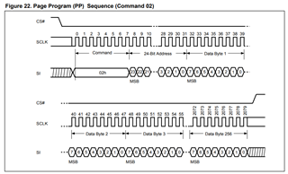
A customer is asking for help on how to use the TMS320F28075 in controlling multiple devices. they want to use the SPI controller in Master mode to make a generic driver where they do the CS using GPIOs. The SPI controller can "control" one CS connection itself but they want to be able to mount multiple devices downstream. the datasheet says in such case that to use GPIO and to code the CS themselves.

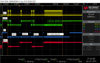
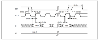
The thing is then when using devices (CHIPS) that require the CS deselect to be at the "edge" where the clock stops pulsing. Any design recommendations on how to achieve that?
Thanks in advance.
Regards,
Marvin
  • Marvin,

    In general, I haven't seen a strict requirement on the deselect timing. Can your customer provide a snapshot of the datasheet requirement?

  • Hi Gus,

    Here is an additional context for the request:

    The customer is currently writing a generic SPI driver for TMS320F28075 and they want to support multiple chips (slaves) downstream but cannot use the built-in CS facility in the SPI controller since it is designed to be used by one slave only. (One can only assign 1 CS pin to the SPI controller).

    The Technical Reference Manual states (paraphrasing) that if using multiple devices (chips) downstream you need to run the CS as GPIOs and control them yourself. The issue is then how to control the CS deselect so it happens at the exact end of the last SPI clock cycle.?

    Does TI have a design proposal or sample code that shows this behavior?

    Can your customer provide a snapshot of the datasheet requirement?

    Datasheet requirement:

    NOR Flash MX25L6433F:
    PP Command (Page Program)

    "The CS# must be kept to low during the whole Page Program cycle; The CS# must go high exactly at the byte
    boundary (the latest eighth bit of data being latched in), otherwise, the instruction will be rejected and will not be
    executed."

    The attached scope image shows a sequence of 4 commands (4 CS) being sent to the nor flash. Since the PP Page Program doesn't work (Consists of sending WREN (Write Enable) first followed by a PP), they surrounded the WREN with a read status register (RDSR) to check the WEL bit (Write Enable Latch). The second RDSR should have produced a high bit in the MISO signal to indicate the WEL bit being set.

    RDSR as per the datasheet does not require "byte shift out boundary" sync with CS deselect.

    I hope this information helps. Please let me know if you needed more information from the customer.

    Regards,

    Marvin

  • Marvin,

    Thanks for providing the extra information. I was able to pull the datasheet. The SPI timing diagram should provide the absolute information on the timing requirements and in this case it doesn't make any sense to me. It shows CS# active/low after the first clock and inactive/high before the last clock. If this is true, it would apply to ALL commands, not just the PP command. I don't see how this is right. I believe your customer should get some clarification from the manufacturer.

    By the way, all the other timing diagrams in the datasheet do not show this.  Below is the diagram for PP for example. It doesn't show this weird CS# requirement.

    If this requirement is true then I don't see a way to meet this requirement using the SPI+GPIO approach. I think the only way to meet this is by bit-banging the SPI signals, i.e. the CPU constructs all the SPI signals using GPIO. However, like I said, I strongly believe there is some typo or misrepresentation on the datasheet spec.

    One common issue we often see when customers use the C2000 SPI is that they program CPOL and CPHA exactly as shown in the slave datasheet. However, manufacturers often define these differently as there is no industry standard definition. I would ask your customer to look at the SPI output and verify the SPI if it is generating the signals to support the flash memory requirement: "For standard single data rate serial mode, input data is latched on the rising edge of Serial Clock(SCLK) and data is shifted out on the falling edge of SCLK." From a C2000 perspective this mode is either CLKPOLARITY = 0 + CLK_PHASE = 1 or CLKPOLARITY = 1 + CLK_PHASE = 0.

  • Hi Gus,

    The customer is doing some investigation and will provide a response by this week.

    I will keep you posted.

    Thanks for the support.

    Regards,

    Marvin