This thread has been locked.

If you have a related question, please click the "Ask a related question" button in the top right corner. The newly created question will be automatically linked to this question.

TMS320F28335: TMS320F28335: PID Simulation (DCL)

Part Number: TMS320F28335

Dear TI members,

I am attaching a code of my simulation for PID. I need your help to just explain parts of the code:

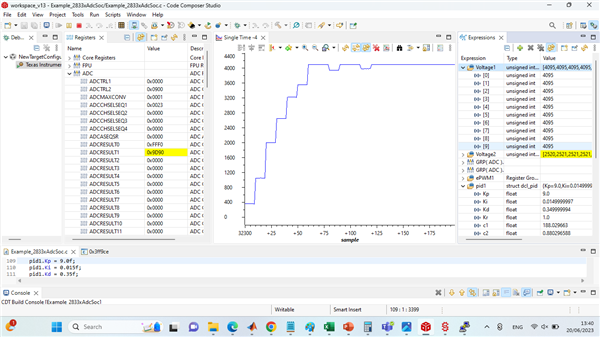
Firstly: If rk =0.25 is set, then yk was achieved with the help of 12 bit ADC values (0-4095) and from the code line 342:

 yk = ((float) AdcRegs.ADCRESULT0 - 2048.0f) / 2047.0f;

yk could be between 1 and -1 .........if (float) AdcRegs.ADCRESULT0 between (4095 and 0). 

Now, next line 345 : uk = DCL_runPID_C4(&pid1, rk, yk, lk);......for running the PID function. which gives Control effort value u(k).

Question1 : Question is what could be the u(k) value range in numbers??? Please explain this line 345.

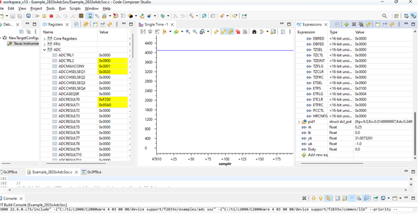
Line 348: clampactive = DCL_runClamp_C1(&uk, upperlim, lowerlim); defining the upper and lower limit saturation. 

Question 2: Line 350: lk = (clampactive == 0U) ? 1.0f : 0.0f;.... There is no compulsion for choosing either 1 or 0 for clampactive. and can we choose any of them????
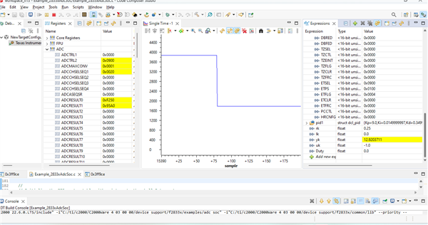
For line 353-354: 

Duty = (uk / 2.0f + 0.5f) * (float) EPwm1Regs.TBPRD;
EPwm1Regs.CMPA.half.CMPA = (Uint16) Duty;

Question3: 

From above line, if u(k) is known from Question 1, then why are we dividing by 2.5 (2.0f+0.5f) and then it multiply with EPwm1Regs.TBPRD ? This Epwm is the one at which we are sampling the ADC at line 286 (EPwm1Regs.TBPRD = 0xFFFF)??? If yes then how this above duty cycle changes if suppose your y(k) changes dues to ADC values? I think I should remove line 309 and then check GPIO0 or GPIO1 to see the change of duty cycle if  y(k) changes.

//###########################################################################
//
// FILE:   Example_2833xAdcSoc.c
//
// TITLE:  ADC Start of Conversion Example
//
//! \addtogroup f2833x_example_list
//! <h1> ADC Start of Conversion (adc_soc)</h1>
//!
//! This ADC example uses ePWM1 to generate a periodic ADC SOC on SEQ1.
//! Two channels are converted, ADCINA3 and ADCINA2.
//!
//! \b Watch \b Variables \n
//! - Voltage1[10]  - Last 10 ADCRESULT0 values
//! - Voltage2[10]  - Last 10 ADCRESULT1 values
//! - ConversionCount   - Current result number 0-9
//! - LoopCount     - Idle loop counter
//
//###########################################################################
// $TI Release: $
// $Release Date: $
// $Copyright:
// Copyright (C) 2009-2023 Texas Instruments Incorporated - http://www.ti.com/
//
// Redistribution and use in source and binary forms, with or without
// modification, are permitted provided that the following conditions
// are met:
//
//   Redistributions of source code must retain the above copyright
//   notice, this list of conditions and the following disclaimer.
//
//   Redistributions in binary form must reproduce the above copyright
//   notice, this list of conditions and the following disclaimer in the
//   documentation and/or other materials provided with the
//   distribution.
//
//   Neither the name of Texas Instruments Incorporated nor the names of
//   its contributors may be used to endorse or promote products derived
//   from this software without specific prior written permission.
//
// THIS SOFTWARE IS PROVIDED BY THE COPYRIGHT HOLDERS AND CONTRIBUTORS
// "AS IS" AND ANY EXPRESS OR IMPLIED WARRANTIES, INCLUDING, BUT NOT
// LIMITED TO, THE IMPLIED WARRANTIES OF MERCHANTABILITY AND FITNESS FOR
// A PARTICULAR PURPOSE ARE DISCLAIMED. IN NO EVENT SHALL THE COPYRIGHT
// OWNER OR CONTRIBUTORS BE LIABLE FOR ANY DIRECT, INDIRECT, INCIDENTAL,
// SPECIAL, EXEMPLARY, OR CONSEQUENTIAL DAMAGES (INCLUDING, BUT NOT
// LIMITED TO, PROCUREMENT OF SUBSTITUTE GOODS OR SERVICES; LOSS OF USE,
// DATA, OR PROFITS; OR BUSINESS INTERRUPTION) HOWEVER CAUSED AND ON ANY
// THEORY OF LIABILITY, WHETHER IN CONTRACT, STRICT LIABILITY, OR TORT
// (INCLUDING NEGLIGENCE OR OTHERWISE) ARISING IN ANY WAY OUT OF THE USE
// OF THIS SOFTWARE, EVEN IF ADVISED OF THE POSSIBILITY OF SUCH DAMAGE.
// $
//###########################################################################

//
// Included Files
//
#include "DSP28x_Project.h"     // Device Headerfile and Examples Include File
#include "DSP2833x_Device.h"
#include "DSP2833x_Examples.h"
#include "DSP2833x_GlobalPrototypes.h"
#include "DCLF32.h"

//
// Function Prototypes
//

void gpio_select(void);
void Setup_ePWM1(void);

__interrupt void adc_isr(void);
//
// Globals
//
Uint16 LoopCount;
Uint16 ConversionCount;
Uint16 Voltage1[10];
Uint16 Voltage2[10];
//DCL_PID pid1 = PID_DEFAULTS;

//typedef struct dcl_pid pid1;

struct dcl_pid pid1;
//float pid1;
DCL_PID pid1 = PID_DEFAULTS;


float32_t yk;
float32_t lk;
float32_t uk;
//float32_t rk = 0.25;                             // initial value for control reference
//float32_t lk = 1.0;                              // control loop not saturated
float32_t rk;                             // initial value for control reference
float32_t lk;                              // control loop not saturated


float Duty;
float upperlim = 0.95;
float lowerlim = 0.05;
unsigned int clampactive;

//
// Main
//

void main(void)
{


    //DCL_PID pid1 = PID_DEFAULTS;

    pid1.Kp = 9.0f;
    pid1.Ki = 0.015f;
    pid1.Kd = 0.35f;
    pid1.Kr = 1.0f;
    pid1.c1 = 188.0296600613396f;
    pid1.c2 = 0.880296600613396f;
    pid1.d2 = 0.0f;
    pid1.d3 = 0.0f;
    pid1.i10 = 0.0f;
    pid1.i14 = 1.0f;
    pid1.Umax = 1.0f;
    pid1.Umin = -1.0f;

    rk = 0.25;                             // initial value for control reference
    lk = 1.0;

    //
    // Step 1. Initialize System Control:
    // PLL, WatchDog, enable Peripheral Clocks
    // This example function is found in the DSP2833x_SysCtrl.c file.
    //
    InitSysCtrl();

    EALLOW;
    #if (CPU_FRQ_150MHZ)     // Default - 150 MHz SYSCLKOUT
        //
        // HSPCLK = SYSCLKOUT/2*ADC_MODCLK2 = 150/(2*3)   = 25.0 MHz
        //
        #define ADC_MODCLK 0x3
    #endif
    #if (CPU_FRQ_100MHZ)
        //
        // HSPCLK = SYSCLKOUT/2*ADC_MODCLK2 = 100/(2*2)   = 25.0 MHz
        //
        #define ADC_MODCLK 0x2
    #endif
    EDIS;

    //
    // Define ADCCLK clock frequency ( less than or equal to 25 MHz )
    // Assuming InitSysCtrl() has set SYSCLKOUT to 150 MHz
    //
    EALLOW;
    SysCtrlRegs.HISPCP.all = ADC_MODCLK;
    EDIS;

    //
    // Step 2. Initialize GPIO:
    // This example function is found in the DSP2833x_Gpio.c file and
    // illustrates how to set the GPIO to it's default state.
    //
    // InitGpio();  // Skipped for this example

    //
    // Step 3. Clear all interrupts and initialize PIE vector table:
    // Disable CPU interrupts
    //
    DINT;

    //
    // Initialize the PIE control registers to their default state.
    // The default state is all PIE interrupts disabled and flags
    // are cleared.
    // This function is found in the DSP2833x_PieCtrl.c file.
    //
    InitPieCtrl();

    //
    // Disable CPU interrupts and clear all CPU interrupt flags:
    //
    IER = 0x0000;
    IFR = 0x0000;

    //
    // Initialize the PIE vector table with pointers to the shell Interrupt
    // Service Routines (ISR).
    // This will populate the entire table, even if the interrupt
    // is not used in this example.  This is useful for debug purposes.
    // The shell ISR routines are found in DSP2833x_DefaultIsr.c.
    // This function is found in DSP2833x_PieVect.c.
    //
    InitPieVectTable();

    //
    // Interrupts that are used in this example are re-mapped to
    // ISR functions found within this file.
    //
    EALLOW;  // This is needed to write to EALLOW protected register
    PieVectTable.ADCINT = &adc_isr;
    EDIS;    // This is needed to disable write to EALLOW protected registers

    //* configure ePWM1 */
    EALLOW;
    SysCtrlRegs.PCLKCR0.bit.TBCLKSYNC = 0;
    EDIS;

    //InitEPwm1Gpio();                             // [F2806x_EPwm.c]
    gpio_select();
    Setup_ePWM1();     // init  ePWM1A


    //void Setup_ePWM1(void)
    //{
    //EPwm1Regs.TBCTL.bit.CTRMODE = 3;        // freeze TB counter
    //EPwm1Regs.TBCTL.bit.PRDLD = 1;          // immediate load
    //EPwm1Regs.TBCTL.bit.PHSEN = 0;          // disable phase loading
    //EPwm1Regs.TBCTL.bit.SYNCOSEL = 3;       // disable SYNCOUT signal
    //EPwm1Regs.TBCTL.bit.HSPCLKDIV = 0;      // TBCLK = SYSCLKOUT
    //EPwm1Regs.TBCTL.bit.CLKDIV = 0;         // clock divider = /1
    //EPwm1Regs.TBCTL.bit.FREE_SOFT = 2;      // free run on emulation suspend
    //EPwm1Regs.TBPRD = 0x2328;               // set period for ePWM1 (0x2328 = 10kHz)
    //EPwm1Regs.TBPHS.all = 0;                // time-base Phase Register
    //EPwm1Regs.TBCTR = 0;                    // time-base Counter Register
    //EPwm1Regs.ETSEL.bit.SOCAEN = 1;         // enable SOC on A group
    //EPwm1Regs.ETSEL.bit.SOCASEL = 1;        // select SOC from zero match
    //EPwm1Regs.ETPS.bit.SOCAPRD = 1;         // generate pulse on 1st event
    //EPwm1Regs.CMPCTL.bit.SHDWAMODE = 0;     // enable shadow mode
    //EPwm1Regs.CMPCTL.bit.LOADAMODE = 2;     // reload on CTR=zero
    //EPwm1Regs.CMPA.half.CMPA = 0x0080;      // set compare A value
    //EPwm1Regs.AQCTLA.bit.CAU = AQ_SET;      // HIGH on CMPA up match
    //EPwm1Regs.AQCTLA.bit.ZRO = AQ_CLEAR;    // LOW on zero match
    //}

    EALLOW;
    SysCtrlRegs.PCLKCR0.bit.TBCLKSYNC = 1;
    EDIS;

    //
    // Step 4. Initialize all the Device Peripherals:
    // This function is found in DSP2833x_InitPeripherals.c
    //
    // InitPeripherals(); // Not required for this example
    InitAdc();  // For this example, init the ADC

    //
    // Step 5. User specific code, enable interrupts:
    //

    //gpio_select();
    //Setup_ePWM1();     // init  ePWM1A,ePWM1B


    //
    // Enable ADCINT in PIE
    //
    PieCtrlRegs.PIEIER1.bit.INTx6 = 1;
    IER |= M_INT1;      // Enable CPU Interrupt 1
    EINT;               // Enable Global interrupt INTM
    ERTM;               // Enable Global realtime interrupt DBGM

    LoopCount = 0;
    ConversionCount = 0;

    //
    // Configure ADC
    //
    AdcRegs.ADCMAXCONV.all = 0x0001;       // Setup 2 conv's on SEQ1
    AdcRegs.ADCCHSELSEQ1.bit.CONV00 = 0x3; // Setup ADCINA3 as 1st SEQ1 conv.
    AdcRegs.ADCCHSELSEQ1.bit.CONV01 = 0x2; // Setup ADCINA2 as 2nd SEQ1 conv.

    //
    // Enable SOCA from ePWM to start SEQ1
    //
    AdcRegs.ADCTRL2.bit.EPWM_SOCA_SEQ1 = 1;

    AdcRegs.ADCTRL2.bit.INT_ENA_SEQ1 = 1;  // Enable SEQ1 interrupt (every EOS)

    //
    // Assumes ePWM1 clock is already enabled in InitSysCtrl();
    //
    EPwm1Regs.ETSEL.bit.SOCAEN = 1;     // Enable SOC on A group
    EPwm1Regs.ETSEL.bit.SOCASEL = 4;    // Select SOC from from CPMA on upcount
    EPwm1Regs.ETPS.bit.SOCAPRD = 1;     // Generate pulse on 1st event
    EPwm1Regs.CMPA.half.CMPA = 0x0080;  // Set compare A value
    EPwm1Regs.TBPRD = 0xFFFF;           // Set period for ePWM1
    EPwm1Regs.TBCTL.bit.CTRMODE = 0;    // count up and start

    //
    // Wait for ADC interrupt
    //
    for(;;)
    {
        LoopCount++;
    }
}

//

void Setup_ePWM1(void)
    {
    EPwm1Regs.TBCTL.bit.CTRMODE = 3;        // freeze TB counter
    EPwm1Regs.TBCTL.bit.PRDLD = 1;          // immediate load
    EPwm1Regs.TBCTL.bit.PHSEN = 0;          // disable phase loading
    EPwm1Regs.TBCTL.bit.SYNCOSEL = 3;       // disable SYNCOUT signal
    EPwm1Regs.TBCTL.bit.HSPCLKDIV = 0;      // TBCLK = SYSCLKOUT
    EPwm1Regs.TBCTL.bit.CLKDIV = 0;         // clock divider = /1
    EPwm1Regs.TBCTL.bit.FREE_SOFT = 2;      // free run on emulation suspend
    EPwm1Regs.TBPRD = 0x2328;               // set period for ePWM1 (0x2328 = 10kHz)
    EPwm1Regs.TBPHS.all = 0;                // time-base Phase Register
    EPwm1Regs.TBCTR = 0;                    // time-base Counter Register
    EPwm1Regs.ETSEL.bit.SOCAEN = 1;         // enable SOC on A group
    EPwm1Regs.ETSEL.bit.SOCASEL = 1;        // select SOC from zero match
    EPwm1Regs.ETPS.bit.SOCAPRD = 1;         // generate pulse on 1st event
    EPwm1Regs.CMPCTL.bit.SHDWAMODE = 0;     // enable shadow mode
    EPwm1Regs.CMPCTL.bit.LOADAMODE = 2;     // reload on CTR=zero
    EPwm1Regs.CMPA.half.CMPA = 0x0080;      // set compare A value
    EPwm1Regs.AQCTLA.bit.CAU = AQ_SET;      // HIGH on CMPA up match
    EPwm1Regs.AQCTLA.bit.ZRO = AQ_CLEAR;    // LOW on zero match
    }


void gpio_select(void)
        {
        EALLOW;
        GpioCtrlRegs.GPAPUD.bit.GPIO0 = 0;   // Enable pullup on GPIO0
        GpioCtrlRegs.GPAPUD.bit.GPIO1 = 0;   // Enable pullup on GPIO1
        GpioCtrlRegs.GPAMUX1.bit.GPIO0 = 1;  // GPIO0 = PWM1A
        GpioCtrlRegs.GPAMUX1.bit.GPIO1 = 1;  // GPIO0 = PWM1B
        EDIS;

        }
// adc_isr -
//
__interrupt void
adc_isr(void)
{
    Voltage1[ConversionCount] = AdcRegs.ADCRESULT0 >>4;
    Voltage2[ConversionCount] = AdcRegs.ADCRESULT1 >>4;

    // read ADC channel
    yk = ((float) AdcRegs.ADCRESULT0 - 2048.0f) / 2047.0f;

    // run PID controller
    uk = DCL_runPID_C4(&pid1, rk, yk, lk);

    // external clamp for anti-windup reset
    clampactive = DCL_runClamp_C1(&uk, upperlim, lowerlim);
    //clampactive = DCL_runClamp_C1(&uk, Umax, Umin);
    lk = (clampactive == 0U) ? 1.0f : 0.0f;

    // write u(k) to PWM
    Duty = (uk / 2.0f + 0.5f) * (float) EPwm1Regs.TBPRD;
    EPwm1Regs.CMPA.half.CMPA = (Uint16) Duty;

    //
    // If 40 conversions have been logged, start over
    //
    if(ConversionCount == 9)
    {
        ConversionCount = 0;
    }
    else
    {
        ConversionCount++;
    }

    //
    // Reinitialize for next ADC sequence
    //
    AdcRegs.ADCTRL2.bit.RST_SEQ1 = 1;         // Reset SEQ1
    AdcRegs.ADCST.bit.INT_SEQ1_CLR = 1;       // Clear INT SEQ1 bit
    PieCtrlRegs.PIEACK.all = PIEACK_GROUP1;   // Acknowledge interrupt to PIE

    return;
}

//
// End of File
//

Please explain all the questions step by step. Sorry I am new to using DCL PID simulation.

Thanks

Regards

Arsalan 

  • Hi Arsalan,

    For Q1, PID controllers also have an internal clamp that is set on line 122&123, therefore, your output ranges will be clamped to 1.0 ~ -1.0

    For Q2, I'm not exactly sure what you meant by "no compulsion for choosing either 1 or 0 for clampactive". The purpose of this external clamp was to make sure that the controller won't be overdamped due to the saturated response (if control effort is clamped) and thus can't be recovered due to the influence of feedback loop. Our example only implemented rudimentary responses to either allow 100% of feedback or 0% of feedback, as shown in this diagram, lk dictates the ratio of the feedback into the controller:

    Feel free to change the values around, and as a matter of fact, this external clamp is unnecessary as PID controller also includes an internal clamp. I believe the purpose of this clamp is only to showcase when lk is clamped. Referring to the code implementation of DCL_PID_C3, which is the inline C version of asm C4.

    For Q3, I would have to reach out to our C2000 PWM export to give you a concrete answer on why are we dividing it by 2.5. But I believe you have some clean up to do as you have multiple instances of EPwm1Regs initialization. Will get to back you later once I received feedback from our internal export.

    Best,

    Sen Wang

  • Hi Seng,

    Thanks for the background information that you have provided. It has been very helpful for me. I will wait for further feedback from you for 2.5 division.

    Yesterday I tested the code on hardware. I am summarizing the results here: Signal is applied at ADCINA3 as input from 0 - 3V setup (see Picture1)

    So here I plotted Voltage 1 graph: that gives a value around 243. at 0.1V ADCINA3 as input voltage and  TBPRD 0xFFFF (see Picture2).

    Picture3 shows all dcl values parameters (Kp,ki,kd,c1,c2,d1,d2.,vmax,vmin...etc). Here rk = 0.25,lk =0,yk=0.9,uk = 0.05 and duty cycle = 34405.875 at 0.1V ADCINA3 as input voltage

    Picture1 :

    Picture 2:  

    Picture 3:

    After increasing the  input voltage ADCINA3 slowly from 0.1V  to 3V, the results are tabulated here in Picture 4 & Picture 5.

    Voltage 1 graph: that gives a value around 4095 in Picture 4. And  rk = 0.25,lk =0,yk=30.9,uk = 0.05 and duty cycle = 34405.875 in Picture5 at 3V ADCINA3 as input voltage

    Picture 4:

    Picture 5:

    Question1: 

    When there is no Power. All ground then, Duty cycle 2.4% at oscilloscope. When Power is up, then Duty cycle 48% . As the input voltage ADCINA3 increases, there is no change in duty cycle number 34405.875 (Picture 5). it remains same and why?  I guess it should change the duty cycle according to the applied voltage change. because I will send this duty cycle to one of ePwm Gpio port to watch the result through oscilloscope to check either the duty cycle changes how much depending upon increasing the applied input voltage. Please explain this. I am following this setup to build on my hardware:


    Question 2: 

    As you see above in above pictures, y(k) is increased from 0.9 to 30.9 when increasing voltage from 0V to 3V ADCINA3 as input voltage.

    In the DCL guide of ''Example 5: PID Controller Running on FPU32'', the y(k) must be equal to r(k) after settling. So here after increasing the input ADCINA3 voltage, the Picture 5 shows the settling output after little delay but y(k) doesn't become equal to reference voltage r(k). Please explain.

    Question3 : 

    c1 and c2 are filter coefficients but d2 and d3 are same as i10 and i14 ? can we say them a coefficient factor after delay? here in above pictures only d2 and d3 are changing when increasing voltage, and why? Please explain.

    Code is attached here: (This time the multiple EPwm1Regs initialization is removed here)

    //###########################################################################
    //
    // FILE:   Example_2833xAdcSoc.c
    //
    // TITLE:  ADC Start of Conversion Example
    //
    //! \addtogroup f2833x_example_list
    //! <h1> ADC Start of Conversion (adc_soc)</h1>
    //!
    //! This ADC example uses ePWM1 to generate a periodic ADC SOC on SEQ1.
    //! Two channels are converted, ADCINA3 and ADCINA2.
    //!
    //! \b Watch \b Variables \n
    //! - Voltage1[10]  - Last 10 ADCRESULT0 values
    //! - Voltage2[10]  - Last 10 ADCRESULT1 values
    //! - ConversionCount   - Current result number 0-9
    //! - LoopCount     - Idle loop counter
    //
    //###########################################################################
    // $TI Release: $
    // $Release Date: $
    // $Copyright:
    // Copyright (C) 2009-2023 Texas Instruments Incorporated - http://www.ti.com/
    //
    // Redistribution and use in source and binary forms, with or without
    // modification, are permitted provided that the following conditions
    // are met:
    //
    //   Redistributions of source code must retain the above copyright
    //   notice, this list of conditions and the following disclaimer.
    //
    //   Redistributions in binary form must reproduce the above copyright
    //   notice, this list of conditions and the following disclaimer in the
    //   documentation and/or other materials provided with the
    //   distribution.
    //
    //   Neither the name of Texas Instruments Incorporated nor the names of
    //   its contributors may be used to endorse or promote products derived
    //   from this software without specific prior written permission.
    //
    // THIS SOFTWARE IS PROVIDED BY THE COPYRIGHT HOLDERS AND CONTRIBUTORS
    // "AS IS" AND ANY EXPRESS OR IMPLIED WARRANTIES, INCLUDING, BUT NOT
    // LIMITED TO, THE IMPLIED WARRANTIES OF MERCHANTABILITY AND FITNESS FOR
    // A PARTICULAR PURPOSE ARE DISCLAIMED. IN NO EVENT SHALL THE COPYRIGHT
    // OWNER OR CONTRIBUTORS BE LIABLE FOR ANY DIRECT, INDIRECT, INCIDENTAL,
    // SPECIAL, EXEMPLARY, OR CONSEQUENTIAL DAMAGES (INCLUDING, BUT NOT
    // LIMITED TO, PROCUREMENT OF SUBSTITUTE GOODS OR SERVICES; LOSS OF USE,
    // DATA, OR PROFITS; OR BUSINESS INTERRUPTION) HOWEVER CAUSED AND ON ANY
    // THEORY OF LIABILITY, WHETHER IN CONTRACT, STRICT LIABILITY, OR TORT
    // (INCLUDING NEGLIGENCE OR OTHERWISE) ARISING IN ANY WAY OUT OF THE USE
    // OF THIS SOFTWARE, EVEN IF ADVISED OF THE POSSIBILITY OF SUCH DAMAGE.
    // $
    //###########################################################################
    
    //
    // Included Files
    //
    #include "DSP28x_Project.h"     // Device Headerfile and Examples Include File
    #include "DSP2833x_Device.h"
    #include "DSP2833x_Examples.h"
    #include "DSP2833x_GlobalPrototypes.h"
    #include "DCLF32.h"
    
    //
    // Function Prototypes
    //
    
    void gpio_select(void);
    void Setup_ePWM1(void);
    
    __interrupt void adc_isr(void);
    //
    // Globals
    //
    Uint16 LoopCount;
    Uint16 ConversionCount;
    Uint16 Voltage1[10];
    Uint16 Voltage2[10];
    
    
    //typedef struct dcl_pid pid1;
    
    struct dcl_pid pid1;
    
    //DCL_PID pid1 = PID_DEFAULTS;
    DCL_PID pid1 = PID_DEFAULTS;
    
    
    float32_t yk;
    float32_t lk;
    float32_t uk;
    float32_t rk;                             // initial value for control reference
    float32_t lk;                              // control loop not saturated
    
    
    float Duty;
    float upperlim = 0.95;
    float lowerlim = 0.05;
    unsigned int clampactive;
    
    //
    // Main
    //
    
    void main(void)
    {
    
    
        pid1.Kp = 9.0f;
        pid1.Ki = 0.015f;
        pid1.Kd = 0.35f;
        pid1.Kr = 1.0f;
        pid1.c1 = 188.0296600613396f;
        pid1.c2 = 0.880296600613396f;
        pid1.d2 = 0.0f;
        pid1.d3 = 0.0f;
        pid1.i10 = 0.0f;
        pid1.i14 = 1.0f;
        pid1.Umax = 1.0f;
        pid1.Umin = -1.0f;
    
        rk = 0.25;               // initial value for control reference
        lk = 1.0;                // control loop not saturated
    
        //
        // Step 1. Initialize System Control:
        // PLL, WatchDog, enable Peripheral Clocks
        // This example function is found in the DSP2833x_SysCtrl.c file.
        //
        InitSysCtrl();
    
        EALLOW;
        #if (CPU_FRQ_150MHZ)     // Default - 150 MHz SYSCLKOUT
            //
            // HSPCLK = SYSCLKOUT/2*ADC_MODCLK2 = 150/(2*3)   = 25.0 MHz
            //
            #define ADC_MODCLK 0x3
        #endif
        #if (CPU_FRQ_100MHZ)
            //
            // HSPCLK = SYSCLKOUT/2*ADC_MODCLK2 = 100/(2*2)   = 25.0 MHz
            //
            #define ADC_MODCLK 0x2
        #endif
        EDIS;
    
        //
        // Define ADCCLK clock frequency ( less than or equal to 25 MHz )
        // Assuming InitSysCtrl() has set SYSCLKOUT to 150 MHz
        //
        EALLOW;
        SysCtrlRegs.HISPCP.all = ADC_MODCLK;
        EDIS;
    
        //
        // Step 2. Initialize GPIO:
        // This example function is found in the DSP2833x_Gpio.c file and
        // illustrates how to set the GPIO to it's default state.
        //
        // InitGpio();  // Skipped for this example
    
        //
        // Step 3. Clear all interrupts and initialize PIE vector table:
        // Disable CPU interrupts
        //
        DINT;
    
        //
        // Initialize the PIE control registers to their default state.
        // The default state is all PIE interrupts disabled and flags
        // are cleared.
        // This function is found in the DSP2833x_PieCtrl.c file.
        //
        InitPieCtrl();
    
        //
        // Disable CPU interrupts and clear all CPU interrupt flags:
        //
        IER = 0x0000;
        IFR = 0x0000;
    
        //
        // Initialize the PIE vector table with pointers to the shell Interrupt
        // Service Routines (ISR).
        // This will populate the entire table, even if the interrupt
        // is not used in this example.  This is useful for debug purposes.
        // The shell ISR routines are found in DSP2833x_DefaultIsr.c.
        // This function is found in DSP2833x_PieVect.c.
        //
        InitPieVectTable();
    
        //
        // Interrupts that are used in this example are re-mapped to
        // ISR functions found within this file.
        //
        EALLOW;  // This is needed to write to EALLOW protected register
        PieVectTable.ADCINT = &adc_isr;
        EDIS;    // This is needed to disable write to EALLOW protected registers
    
        //* configure ePWM1 */
        EALLOW;
        SysCtrlRegs.PCLKCR0.bit.TBCLKSYNC = 0;
        EDIS;
    
        //InitEPwm1Gpio();                             // [F2806x_EPwm.c]
        gpio_select();
        Setup_ePWM1();     // init  ePWM1A
    
        EALLOW;
        SysCtrlRegs.PCLKCR0.bit.TBCLKSYNC = 1;
        EDIS;
    
        //
        // Step 4. Initialize all the Device Peripherals:
        // This function is found in DSP2833x_InitPeripherals.c
        //
        // InitPeripherals(); // Not required for this example
        InitAdc();  // For this example, init the ADC
    
        //
        // Step 5. User specific code, enable interrupts:
        //
    
        //
        // Enable ADCINT in PIE
        //
        PieCtrlRegs.PIEIER1.bit.INTx6 = 1;
        IER |= M_INT1;      // Enable CPU Interrupt 1
        EINT;               // Enable Global interrupt INTM
        ERTM;               // Enable Global realtime interrupt DBGM
    
        LoopCount = 0;
        ConversionCount = 0;
    
        //
        // Configure ADC
        //
        AdcRegs.ADCMAXCONV.all = 0x0001;       // Setup 2 conv's on SEQ1
        AdcRegs.ADCCHSELSEQ1.bit.CONV00 = 0x3; // Setup ADCINA3 as 1st SEQ1 conv.
        AdcRegs.ADCCHSELSEQ1.bit.CONV01 = 0x2; // Setup ADCINA2 as 2nd SEQ1 conv.
    
        //
        // Enable SOCA from ePWM to start SEQ1
        //
        AdcRegs.ADCTRL2.bit.EPWM_SOCA_SEQ1 = 1;
    
        AdcRegs.ADCTRL2.bit.INT_ENA_SEQ1 = 1;  // Enable SEQ1 interrupt (every EOS)
    
        //
        // Assumes ePWM1 clock is already enabled in InitSysCtrl();
    
        //
        // Wait for ADC interrupt
        //
        for(;;)
        {
            LoopCount++;
        }
    }
    
    //
    
    void Setup_ePWM1(void)
        {
        //EPwm1Regs.TBCTL.bit.CTRMODE = 3;        // freeze TB counter
        EPwm1Regs.TBCTL.bit.CTRMODE = 0;        // count up and start
        EPwm1Regs.TBCTL.bit.PRDLD = 1;          // immediate load
        EPwm1Regs.TBCTL.bit.PHSEN = 0;          // disable phase loading
        EPwm1Regs.TBCTL.bit.SYNCOSEL = 3;       // disable SYNCOUT signal
        EPwm1Regs.TBCTL.bit.HSPCLKDIV = 0;      // TBCLK = SYSCLKOUT
        EPwm1Regs.TBCTL.bit.CLKDIV = 0;         // clock divider = /1
        EPwm1Regs.TBCTL.bit.FREE_SOFT = 2;      // free run on emulation suspend
        //EPwm1Regs.TBPRD = 0x2328;               // set period for ePWM1 (0x2328 = 10kHz)
        EPwm1Regs.TBPRD = 0xFFFF;               // set period for ePWM1 (0x2328 = 10kHz)
        EPwm1Regs.TBPHS.all = 0;                // time-base Phase Register
        EPwm1Regs.TBCTR = 0;                    // time-base Counter Register
        EPwm1Regs.ETSEL.bit.SOCAEN = 1;         // enable SOC on A group
        //EPwm1Regs.ETSEL.bit.SOCASEL = 1;        // select SOC from zero match
        EPwm1Regs.ETSEL.bit.SOCASEL = 1;        // select SOC from zero match
        //EPwm1Regs.ETSEL.bit.SOCASEL = 4;        // select SOC from zero match
        EPwm1Regs.ETPS.bit.SOCAPRD = 1;         // generate pulse on 1st event
        EPwm1Regs.CMPCTL.bit.SHDWAMODE = 0;     // enable shadow mode
        EPwm1Regs.CMPCTL.bit.LOADAMODE = 2;     // reload on CTR=zero
        EPwm1Regs.CMPA.half.CMPA = 0x0080;      // set compare A value
        EPwm1Regs.AQCTLA.bit.CAU = AQ_SET;      // HIGH on CMPA up match
        EPwm1Regs.AQCTLA.bit.ZRO = AQ_CLEAR;    // LOW on zero match
        }
    
    
    void gpio_select(void)
            {
            EALLOW;
            GpioCtrlRegs.GPAPUD.bit.GPIO0 = 0;   // Enable pullup on GPIO0
            GpioCtrlRegs.GPAPUD.bit.GPIO1 = 0;   // Enable pullup on GPIO1
            GpioCtrlRegs.GPAMUX1.bit.GPIO0 = 1;  // GPIO0 = PWM1A
            GpioCtrlRegs.GPAMUX1.bit.GPIO1 = 1;  // GPIO0 = PWM1B
            EDIS;
    
            }
    // adc_isr -
    //
    __interrupt void
    adc_isr(void)
    {
        Voltage1[ConversionCount] = AdcRegs.ADCRESULT0 >>4;
        Voltage2[ConversionCount] = AdcRegs.ADCRESULT1 >>4;
    
        // read ADC channel
        yk = ((float) AdcRegs.ADCRESULT0 - 2048.0f) / 2047.0f;
    
        // run PID controller
        uk = DCL_runPID_C4(&pid1, rk, yk, lk);
    
        // external clamp for anti-windup reset
        clampactive = DCL_runClamp_C1(&uk, upperlim, lowerlim);
        //clampactive = DCL_runClamp_C1(&uk, Umax, Umin);
        lk = (clampactive == 0U) ? 1.0f : 0.0f;
    
        // write u(k) to PWM
        Duty = (uk / 2.0f + 0.5f) * (float) EPwm1Regs.TBPRD;
        EPwm1Regs.CMPA.half.CMPA = (Uint16) Duty;
    
        //
        // If 40 conversions have been logged, start over
        //
        if(ConversionCount == 9)
        {
            ConversionCount = 0;
        }
        else
        {
            ConversionCount++;
        }
    
        //
        // Reinitialize for next ADC sequence
        //
        AdcRegs.ADCTRL2.bit.RST_SEQ1 = 1;         // Reset SEQ1
        AdcRegs.ADCST.bit.INT_SEQ1_CLR = 1;       // Clear INT SEQ1 bit
        PieCtrlRegs.PIEACK.all = PIEACK_GROUP1;   // Acknowledge interrupt to PIE
    
        return;
    }
    
    //
    // End of File
    //


    Thanks

    Regards

    Arsalan  

  • I will wait for further feedback from you for 2.5 division.

    Hi Arsalan,

    This is line is NOT dividing by 2.5f. Instead it's explained by this thread: e2e.ti.com/.../ccs-tms320f28379d-dcl-c200-motorware

    "In response to the first question, the assumption in the example was that the controller output was normalised to +/-1.0f. The code line scales and then offsets the controller output to bring it in the 0 - 1.0f range, which is multiplied by the PWM period to get the duty cycle. It's just a code example."

    Best regards,

    Ryan Ma

  • Hi Arsalan, I apologize for the delay.

    Like Ryan said, uk/2.0f + 0.5f was an attempt to normalize the control output range from -1.0~1.0f to 0~1.0f, representing 0% to 100% of the duty cycle.

    And judging from your code, you've setup ADCINA2, ADCINA3 on F28335 but the ISR is still reading ADCRESULT0 from the F28069 DCL example, providing the signal to ADCINA3 shouldn't have any effect on ADCRESULT0 and all subsequent changes in ADCRESULT0 and PID is probably due to floating voltages. 

    One thing I forgot to mention is that there's also an external saturation that is included to further clamp the saturation range to 0.05f~0.95f instead of +/-1.0f. So you could comment out the runClamp_C1 in line 315 if you don't need additional saturation.

    Best,

    Sen Wang

  • Hi Ryan,

    Thanks for your reply. I will get back to you soon after implementing your suggestion. I will let you know the results soon.

    Regards

    Arsalan

  • Hi Sen,

    Thanks for your reply. I will get back to you soon after implementing your suggestion. I will let you know the results soon.

    Regards

    Arsalan

  • We will await your results.

    Best,

    Ryan Ma

  • Hi Sen & Ryan,

    Thanks for your comprehensive replies. Quite Helpful

    And judging from your code, you've setup ADCINA2, ADCINA3 on F28335 but the ISR is still reading ADCRESULT0 from the F28069 DCL example, providing the signal to ADCINA3 shouldn't have any effect on ADCRESULT0 and all subsequent changes in ADCRESULT0 and PID is probably due to floating voltages. 

    As suggested, I fixed that issue, Now I am applying at ADCINA0 and ISR is reading ADCRESULT. and it is reading the duty cycle only at 2 values. (65553 or 0) at 0V and 3V respectively on watch window. There is no middle value it gives when i set the voltage suppose 1.2V and the duty cycle is 0 (no middle value around). see Picture. below:

    At 0V(ground) applied on ADCINA0, the output Voltage1 = 0 approx on watch window, The Duty is 65535.(because TBPRD = FFFF) see Picture 1,2 and when 3V applied, the Duty cycle shows 0 Picture 3,4.

    Picture 5 shows that when i applied a voltage of 1.2 approx at  ADCINA0, the Duty cycle doesn't show around a middle value. it stays at 0. The Duty cycle must be change depending upon the whatever the voltage is applied accordingly.

    Picture1 (at 0 V)

    Picture2 (at 0V)--Duty cycle = 65535


    Picture3 (at 3 V)

    Picture4 (at 3V)--Duty cycle = 0

    Picture 5 (at 1.2V approx)... Duty cycle has no middle value. it stays at 0.

    Updated code is attached here

    //###########################################################################
    //
    // FILE:   Example_2833xAdcSoc.c
    //
    // TITLE:  ADC Start of Conversion Example
    //
    //! \addtogroup f2833x_example_list
    //! <h1> ADC Start of Conversion (adc_soc)</h1>
    //!
    //! This ADC example uses ePWM1 to generate a periodic ADC SOC on SEQ1.
    //! Two channels are converted, ADCINA3 and ADCINA2.
    //!
    //! \b Watch \b Variables \n
    //! - Voltage1[10]  - Last 10 ADCRESULT0 values
    //! - Voltage2[10]  - Last 10 ADCRESULT1 values
    //! - ConversionCount   - Current result number 0-9
    //! - LoopCount     - Idle loop counter
    //
    //###########################################################################
    // $TI Release: $
    // $Release Date: $
    // $Copyright:
    // Copyright (C) 2009-2023 Texas Instruments Incorporated - http://www.ti.com/
    //
    // Redistribution and use in source and binary forms, with or without
    // modification, are permitted provided that the following conditions
    // are met:
    //
    //   Redistributions of source code must retain the above copyright
    //   notice, this list of conditions and the following disclaimer.
    //
    //   Redistributions in binary form must reproduce the above copyright
    //   notice, this list of conditions and the following disclaimer in the
    //   documentation and/or other materials provided with the
    //   distribution.
    //
    //   Neither the name of Texas Instruments Incorporated nor the names of
    //   its contributors may be used to endorse or promote products derived
    //   from this software without specific prior written permission.
    //
    // THIS SOFTWARE IS PROVIDED BY THE COPYRIGHT HOLDERS AND CONTRIBUTORS
    // "AS IS" AND ANY EXPRESS OR IMPLIED WARRANTIES, INCLUDING, BUT NOT
    // LIMITED TO, THE IMPLIED WARRANTIES OF MERCHANTABILITY AND FITNESS FOR
    // A PARTICULAR PURPOSE ARE DISCLAIMED. IN NO EVENT SHALL THE COPYRIGHT
    // OWNER OR CONTRIBUTORS BE LIABLE FOR ANY DIRECT, INDIRECT, INCIDENTAL,
    // SPECIAL, EXEMPLARY, OR CONSEQUENTIAL DAMAGES (INCLUDING, BUT NOT
    // LIMITED TO, PROCUREMENT OF SUBSTITUTE GOODS OR SERVICES; LOSS OF USE,
    // DATA, OR PROFITS; OR BUSINESS INTERRUPTION) HOWEVER CAUSED AND ON ANY
    // THEORY OF LIABILITY, WHETHER IN CONTRACT, STRICT LIABILITY, OR TORT
    // (INCLUDING NEGLIGENCE OR OTHERWISE) ARISING IN ANY WAY OUT OF THE USE
    // OF THIS SOFTWARE, EVEN IF ADVISED OF THE POSSIBILITY OF SUCH DAMAGE.
    // $
    //###########################################################################
    
    //
    // Included Files
    //
    #include "DSP28x_Project.h"     // Device Headerfile and Examples Include File
    #include "DSP2833x_Device.h"
    #include "DSP2833x_Examples.h"
    #include "DSP2833x_GlobalPrototypes.h"
    #include "DCLF32.h"
    
    //
    // Function Prototypes
    //
    
    void gpio_select(void);
    void Setup_ePWM1(void);
    
    __interrupt void adc_isr(void);
    //
    // Globals
    //
    Uint16 LoopCount;
    Uint16 ConversionCount;
    Uint16 Voltage1[10];
    Uint16 Voltage2[10];
    
    
    //typedef struct dcl_pid pid1;
    
    struct dcl_pid pid1;
    
    //DCL_PID pid1 = PID_DEFAULTS;
    DCL_PID pid1 = PID_DEFAULTS;
    
    
    float32_t yk;
    float32_t lk;
    float32_t uk;
    float32_t rk;                             // initial value for control reference
    float32_t lk;                              // control loop not saturated
    
    
    float Duty;
    float upperlim = 0.95;
    float lowerlim = 0.05;
    unsigned int clampactive;
    
    //
    // Main
    //
    
    void main(void)
    {
    
    
        pid1.Kp = 9.0f;
        pid1.Ki = 0.015f;
        pid1.Kd = 0.35f;
        pid1.Kr = 1.0f;
        pid1.c1 = 188.0296600613396f;
        pid1.c2 = 0.880296600613396f;
        pid1.d2 = 0.0f;
        pid1.d3 = 0.0f;
        pid1.i10 = 0.0f;
        pid1.i14 = 1.0f;
        pid1.Umax = 1.0f;
        pid1.Umin = -1.0f;
    
        rk = 0.25;               // initial value for control reference
        lk = 1.0;                // control loop not saturated
    
        //
        // Step 1. Initialize System Control:
        // PLL, WatchDog, enable Peripheral Clocks
        // This example function is found in the DSP2833x_SysCtrl.c file.
        //
        InitSysCtrl();
    
        EALLOW;
        #if (CPU_FRQ_150MHZ)     // Default - 150 MHz SYSCLKOUT
            //
            // HSPCLK = SYSCLKOUT/2*ADC_MODCLK2 = 150/(2*3)   = 25.0 MHz
            //
            #define ADC_MODCLK 0x3
        #endif
        #if (CPU_FRQ_100MHZ)
            //
            // HSPCLK = SYSCLKOUT/2*ADC_MODCLK2 = 100/(2*2)   = 25.0 MHz
            //
            #define ADC_MODCLK 0x2
        #endif
        EDIS;
    
        //
        // Define ADCCLK clock frequency ( less than or equal to 25 MHz )
        // Assuming InitSysCtrl() has set SYSCLKOUT to 150 MHz
        //
        EALLOW;
        SysCtrlRegs.HISPCP.all = ADC_MODCLK;
        EDIS;
    
        //
        // Step 2. Initialize GPIO:
        // This example function is found in the DSP2833x_Gpio.c file and
        // illustrates how to set the GPIO to it's default state.
        //
        // InitGpio();  // Skipped for this example
    
        //
        // Step 3. Clear all interrupts and initialize PIE vector table:
        // Disable CPU interrupts
        //
        DINT;
    
        //
        // Initialize the PIE control registers to their default state.
        // The default state is all PIE interrupts disabled and flags
        // are cleared.
        // This function is found in the DSP2833x_PieCtrl.c file.
        //
        InitPieCtrl();
    
        //
        // Disable CPU interrupts and clear all CPU interrupt flags:
        //
        IER = 0x0000;
        IFR = 0x0000;
    
        //
        // Initialize the PIE vector table with pointers to the shell Interrupt
        // Service Routines (ISR).
        // This will populate the entire table, even if the interrupt
        // is not used in this example.  This is useful for debug purposes.
        // The shell ISR routines are found in DSP2833x_DefaultIsr.c.
        // This function is found in DSP2833x_PieVect.c.
        //
        InitPieVectTable();
    
        //
        // Interrupts that are used in this example are re-mapped to
        // ISR functions found within this file.
        //
        EALLOW;  // This is needed to write to EALLOW protected register
        PieVectTable.ADCINT = &adc_isr;
        EDIS;    // This is needed to disable write to EALLOW protected registers
    
        //* configure ePWM1 */
        EALLOW;
        SysCtrlRegs.PCLKCR0.bit.TBCLKSYNC = 0;
        EDIS;
    
        //InitEPwm1Gpio();                             // [F2806x_EPwm.c]
        gpio_select();
        Setup_ePWM1();     // init  ePWM1A
    
        EALLOW;
        SysCtrlRegs.PCLKCR0.bit.TBCLKSYNC = 1;
        EDIS;
    
        //
        // Step 4. Initialize all the Device Peripherals:
        // This function is found in DSP2833x_InitPeripherals.c
        //
        // InitPeripherals(); // Not required for this example
        InitAdc();  // For this example, init the ADC
    
        //
        // Step 5. User specific code, enable interrupts:
        //
    
        //
        // Enable ADCINT in PIE
        //
        PieCtrlRegs.PIEIER1.bit.INTx6 = 1;
        IER |= M_INT1;      // Enable CPU Interrupt 1
        EINT;               // Enable Global interrupt INTM
        ERTM;               // Enable Global realtime interrupt DBGM
    
        LoopCount = 0;
        ConversionCount = 0;
    
        //
        // Configure ADC
        //
        AdcRegs.ADCMAXCONV.all = 0x0001;       // Setup 2 conv's on SEQ1
        AdcRegs.ADCCHSELSEQ1.bit.CONV00 = 0x0; // Setup ADCINA0 as 1st SEQ1 conv.
        AdcRegs.ADCCHSELSEQ1.bit.CONV01 = 0x2; // Setup ADCINA2 as 2nd SEQ1 conv.
    
        //
        // Enable SOCA from ePWM to start SEQ1
        //
        AdcRegs.ADCTRL2.bit.EPWM_SOCA_SEQ1 = 1;
    
        AdcRegs.ADCTRL2.bit.INT_ENA_SEQ1 = 1;  // Enable SEQ1 interrupt (every EOS)
    
        //
        // Assumes ePWM1 clock is already enabled in InitSysCtrl();
    
        //
        // Wait for ADC interrupt
        //
        for(;;)
        {
            LoopCount++;
        }
    }
    
    //
    
    void Setup_ePWM1(void)
        {
        //EPwm1Regs.TBCTL.bit.CTRMODE = 3;        // freeze TB counter
        EPwm1Regs.TBCTL.bit.CTRMODE = 0;        // count up and start
        EPwm1Regs.TBCTL.bit.PRDLD = 1;          // immediate load
        EPwm1Regs.TBCTL.bit.PHSEN = 0;          // disable phase loading
        EPwm1Regs.TBCTL.bit.SYNCOSEL = 3;       // disable SYNCOUT signal
        EPwm1Regs.TBCTL.bit.HSPCLKDIV = 0;      // TBCLK = SYSCLKOUT
        EPwm1Regs.TBCTL.bit.CLKDIV = 0;         // clock divider = /1
        EPwm1Regs.TBCTL.bit.FREE_SOFT = 2;      // free run on emulation suspend
        //EPwm1Regs.TBPRD = 0x2328;               // set period for ePWM1 (0x2328 = 10kHz)
        EPwm1Regs.TBPRD = 0xFFFF;               // set period for ePWM1 (0x2328 = 10kHz)
        EPwm1Regs.TBPHS.all = 0;                // time-base Phase Register
        EPwm1Regs.TBCTR = 0;                    // time-base Counter Register
        EPwm1Regs.ETSEL.bit.SOCAEN = 1;         // enable SOC on A group
        //EPwm1Regs.ETSEL.bit.SOCASEL = 1;        // select SOC from zero match
        EPwm1Regs.ETSEL.bit.SOCASEL = 1;        // select SOC from zero match
        //EPwm1Regs.ETSEL.bit.SOCASEL = 4;        // select SOC from zero match
        EPwm1Regs.ETPS.bit.SOCAPRD = 1;         // generate pulse on 1st event
        EPwm1Regs.CMPCTL.bit.SHDWAMODE = 0;     // enable shadow mode
        EPwm1Regs.CMPCTL.bit.LOADAMODE = 2;     // reload on CTR=zero
        EPwm1Regs.CMPA.half.CMPA = 0x0080;      // set compare A value
        EPwm1Regs.AQCTLA.bit.CAU = AQ_SET;      // HIGH on CMPA up match
        EPwm1Regs.AQCTLA.bit.ZRO = AQ_CLEAR;    // LOW on zero match
        }
    
    
    void gpio_select(void)
            {
            EALLOW;
            GpioCtrlRegs.GPAPUD.bit.GPIO0 = 0;   // Enable pullup on GPIO0
            GpioCtrlRegs.GPAPUD.bit.GPIO1 = 0;   // Enable pullup on GPIO1
            GpioCtrlRegs.GPAMUX1.bit.GPIO0 = 1;  // GPIO0 = PWM1A
            GpioCtrlRegs.GPAMUX1.bit.GPIO1 = 1;  // GPIO0 = PWM1B
            EDIS;
    
            }
    // adc_isr -
    //
    __interrupt void
    adc_isr(void)
    {
        Voltage1[ConversionCount] = AdcRegs.ADCRESULT0 >>4;
        Voltage2[ConversionCount] = AdcRegs.ADCRESULT1 >>4;
    
        // read ADC channel
        yk = ((float) AdcRegs.ADCRESULT0 - 2048.0f) / 2047.0f;
    
        // run PID controller
        uk = DCL_runPID_C4(&pid1, rk, yk, lk);
    
        // external clamp for anti-windup reset
        //clampactive = DCL_runClamp_C1(&uk, upperlim, lowerlim);
        //clampactive = DCL_runClamp_C1(&uk, Umax, Umin);
        lk = (clampactive == 0U) ? 1.0f : 0.0f;
    
        // write u(k) to PWM
        Duty = (uk / 2.0f + 0.5f) * (float) EPwm1Regs.TBPRD;
        EPwm1Regs.CMPA.half.CMPA = (Uint16) Duty;
    
        //
        // If 40 conversions have been logged, start over
        //
        if(ConversionCount == 9)
        {
            ConversionCount = 0;
        }
        else
        {
            ConversionCount++;
        }
    
        //
        // Reinitialize for next ADC sequence
        //
        AdcRegs.ADCTRL2.bit.RST_SEQ1 = 1;         // Reset SEQ1
        AdcRegs.ADCST.bit.INT_SEQ1_CLR = 1;       // Clear INT SEQ1 bit
        PieCtrlRegs.PIEACK.all = PIEACK_GROUP1;   // Acknowledge interrupt to PIE
    
        return;
    }
    
    //
    // End of File
    //
    

    Please suggest this issue accordingly

    Thanks

    Regards

    Arsalan

  • Hi Sen & Ryan,

    Thanks for your comprehensive replies. Quite Helpful

    And judging from your code, you've setup ADCINA2, ADCINA3 on F28335 but the ISR is still reading ADCRESULT0 from the F28069 DCL example, providing the signal to ADCINA3 shouldn't have any effect on ADCRESULT0 and all subsequent changes in ADCRESULT0 and PID is probably due to floating voltages. 

    As suggested, I fixed that issue, Now I am applying at ADCINA0 and ISR is reading ADCRESULT. and it is reading the duty cycle only at 2 values. (65553 or 0) at 0V and 3V respectively on watch window. There is no middle value it gives when i set the voltage suppose 1.2V and the duty cycle is 0 (no middle value around). see Picture. below:

    At 0V(ground) applied on ADCINA0, the output Voltage1 = 0 approx on watch window, The Duty is 65535.(because TBPRD = FFFF) see Picture 1,2 and when 3V applied, the Duty cycle shows 0 Picture 3,4.

    Picture 5 shows that when i applied a voltage of 1.2 approx at  ADCINA0, the Duty cycle doesn't show around a middle value. it stays at 0. The Duty cycle must be change depending upon the whatever the voltage is applied accordingly.

    Picture1 (at 0 V)

    Picture2 (at 0V)--Duty cycle = 65535


    Picture3 (at 3 V)

    Picture4 (at 3V)--Duty cycle = 0

    Picture 5 (at 1.2V approx)... Duty cycle has no middle value. it stays at 0.

    Updated code is attached here

    //###########################################################################
    //
    // FILE:   Example_2833xAdcSoc.c
    //
    // TITLE:  ADC Start of Conversion Example
    //
    //! \addtogroup f2833x_example_list
    //! <h1> ADC Start of Conversion (adc_soc)</h1>
    //!
    //! This ADC example uses ePWM1 to generate a periodic ADC SOC on SEQ1.
    //! Two channels are converted, ADCINA3 and ADCINA2.
    //!
    //! \b Watch \b Variables \n
    //! - Voltage1[10]  - Last 10 ADCRESULT0 values
    //! - Voltage2[10]  - Last 10 ADCRESULT1 values
    //! - ConversionCount   - Current result number 0-9
    //! - LoopCount     - Idle loop counter
    //
    //###########################################################################
    // $TI Release: $
    // $Release Date: $
    // $Copyright:
    // Copyright (C) 2009-2023 Texas Instruments Incorporated - http://www.ti.com/
    //
    // Redistribution and use in source and binary forms, with or without
    // modification, are permitted provided that the following conditions
    // are met:
    //
    //   Redistributions of source code must retain the above copyright
    //   notice, this list of conditions and the following disclaimer.
    //
    //   Redistributions in binary form must reproduce the above copyright
    //   notice, this list of conditions and the following disclaimer in the
    //   documentation and/or other materials provided with the
    //   distribution.
    //
    //   Neither the name of Texas Instruments Incorporated nor the names of
    //   its contributors may be used to endorse or promote products derived
    //   from this software without specific prior written permission.
    //
    // THIS SOFTWARE IS PROVIDED BY THE COPYRIGHT HOLDERS AND CONTRIBUTORS
    // "AS IS" AND ANY EXPRESS OR IMPLIED WARRANTIES, INCLUDING, BUT NOT
    // LIMITED TO, THE IMPLIED WARRANTIES OF MERCHANTABILITY AND FITNESS FOR
    // A PARTICULAR PURPOSE ARE DISCLAIMED. IN NO EVENT SHALL THE COPYRIGHT
    // OWNER OR CONTRIBUTORS BE LIABLE FOR ANY DIRECT, INDIRECT, INCIDENTAL,
    // SPECIAL, EXEMPLARY, OR CONSEQUENTIAL DAMAGES (INCLUDING, BUT NOT
    // LIMITED TO, PROCUREMENT OF SUBSTITUTE GOODS OR SERVICES; LOSS OF USE,
    // DATA, OR PROFITS; OR BUSINESS INTERRUPTION) HOWEVER CAUSED AND ON ANY
    // THEORY OF LIABILITY, WHETHER IN CONTRACT, STRICT LIABILITY, OR TORT
    // (INCLUDING NEGLIGENCE OR OTHERWISE) ARISING IN ANY WAY OUT OF THE USE
    // OF THIS SOFTWARE, EVEN IF ADVISED OF THE POSSIBILITY OF SUCH DAMAGE.
    // $
    //###########################################################################
    
    //
    // Included Files
    //
    #include "DSP28x_Project.h"     // Device Headerfile and Examples Include File
    #include "DSP2833x_Device.h"
    #include "DSP2833x_Examples.h"
    #include "DSP2833x_GlobalPrototypes.h"
    #include "DCLF32.h"
    
    //
    // Function Prototypes
    //
    
    void gpio_select(void);
    void Setup_ePWM1(void);
    
    __interrupt void adc_isr(void);
    //
    // Globals
    //
    Uint16 LoopCount;
    Uint16 ConversionCount;
    Uint16 Voltage1[10];
    Uint16 Voltage2[10];
    
    
    //typedef struct dcl_pid pid1;
    
    struct dcl_pid pid1;
    
    //DCL_PID pid1 = PID_DEFAULTS;
    DCL_PID pid1 = PID_DEFAULTS;
    
    
    float32_t yk;
    float32_t lk;
    float32_t uk;
    float32_t rk;                             // initial value for control reference
    float32_t lk;                              // control loop not saturated
    
    
    float Duty;
    float upperlim = 0.95;
    float lowerlim = 0.05;
    unsigned int clampactive;
    
    //
    // Main
    //
    
    void main(void)
    {
    
    
        pid1.Kp = 9.0f;
        pid1.Ki = 0.015f;
        pid1.Kd = 0.35f;
        pid1.Kr = 1.0f;
        pid1.c1 = 188.0296600613396f;
        pid1.c2 = 0.880296600613396f;
        pid1.d2 = 0.0f;
        pid1.d3 = 0.0f;
        pid1.i10 = 0.0f;
        pid1.i14 = 1.0f;
        pid1.Umax = 1.0f;
        pid1.Umin = -1.0f;
    
        rk = 0.25;               // initial value for control reference
        lk = 1.0;                // control loop not saturated
    
        //
        // Step 1. Initialize System Control:
        // PLL, WatchDog, enable Peripheral Clocks
        // This example function is found in the DSP2833x_SysCtrl.c file.
        //
        InitSysCtrl();
    
        EALLOW;
        #if (CPU_FRQ_150MHZ)     // Default - 150 MHz SYSCLKOUT
            //
            // HSPCLK = SYSCLKOUT/2*ADC_MODCLK2 = 150/(2*3)   = 25.0 MHz
            //
            #define ADC_MODCLK 0x3
        #endif
        #if (CPU_FRQ_100MHZ)
            //
            // HSPCLK = SYSCLKOUT/2*ADC_MODCLK2 = 100/(2*2)   = 25.0 MHz
            //
            #define ADC_MODCLK 0x2
        #endif
        EDIS;
    
        //
        // Define ADCCLK clock frequency ( less than or equal to 25 MHz )
        // Assuming InitSysCtrl() has set SYSCLKOUT to 150 MHz
        //
        EALLOW;
        SysCtrlRegs.HISPCP.all = ADC_MODCLK;
        EDIS;
    
        //
        // Step 2. Initialize GPIO:
        // This example function is found in the DSP2833x_Gpio.c file and
        // illustrates how to set the GPIO to it's default state.
        //
        // InitGpio();  // Skipped for this example
    
        //
        // Step 3. Clear all interrupts and initialize PIE vector table:
        // Disable CPU interrupts
        //
        DINT;
    
        //
        // Initialize the PIE control registers to their default state.
        // The default state is all PIE interrupts disabled and flags
        // are cleared.
        // This function is found in the DSP2833x_PieCtrl.c file.
        //
        InitPieCtrl();
    
        //
        // Disable CPU interrupts and clear all CPU interrupt flags:
        //
        IER = 0x0000;
        IFR = 0x0000;
    
        //
        // Initialize the PIE vector table with pointers to the shell Interrupt
        // Service Routines (ISR).
        // This will populate the entire table, even if the interrupt
        // is not used in this example.  This is useful for debug purposes.
        // The shell ISR routines are found in DSP2833x_DefaultIsr.c.
        // This function is found in DSP2833x_PieVect.c.
        //
        InitPieVectTable();
    
        //
        // Interrupts that are used in this example are re-mapped to
        // ISR functions found within this file.
        //
        EALLOW;  // This is needed to write to EALLOW protected register
        PieVectTable.ADCINT = &adc_isr;
        EDIS;    // This is needed to disable write to EALLOW protected registers
    
        //* configure ePWM1 */
        EALLOW;
        SysCtrlRegs.PCLKCR0.bit.TBCLKSYNC = 0;
        EDIS;
    
        //InitEPwm1Gpio();                             // [F2806x_EPwm.c]
        gpio_select();
        Setup_ePWM1();     // init  ePWM1A
    
        EALLOW;
        SysCtrlRegs.PCLKCR0.bit.TBCLKSYNC = 1;
        EDIS;
    
        //
        // Step 4. Initialize all the Device Peripherals:
        // This function is found in DSP2833x_InitPeripherals.c
        //
        // InitPeripherals(); // Not required for this example
        InitAdc();  // For this example, init the ADC
    
        //
        // Step 5. User specific code, enable interrupts:
        //
    
        //
        // Enable ADCINT in PIE
        //
        PieCtrlRegs.PIEIER1.bit.INTx6 = 1;
        IER |= M_INT1;      // Enable CPU Interrupt 1
        EINT;               // Enable Global interrupt INTM
        ERTM;               // Enable Global realtime interrupt DBGM
    
        LoopCount = 0;
        ConversionCount = 0;
    
        //
        // Configure ADC
        //
        AdcRegs.ADCMAXCONV.all = 0x0001;       // Setup 2 conv's on SEQ1
        AdcRegs.ADCCHSELSEQ1.bit.CONV00 = 0x0; // Setup ADCINA0 as 1st SEQ1 conv.
        AdcRegs.ADCCHSELSEQ1.bit.CONV01 = 0x2; // Setup ADCINA2 as 2nd SEQ1 conv.
    
        //
        // Enable SOCA from ePWM to start SEQ1
        //
        AdcRegs.ADCTRL2.bit.EPWM_SOCA_SEQ1 = 1;
    
        AdcRegs.ADCTRL2.bit.INT_ENA_SEQ1 = 1;  // Enable SEQ1 interrupt (every EOS)
    
        //
        // Assumes ePWM1 clock is already enabled in InitSysCtrl();
    
        //
        // Wait for ADC interrupt
        //
        for(;;)
        {
            LoopCount++;
        }
    }
    
    //
    
    void Setup_ePWM1(void)
        {
        //EPwm1Regs.TBCTL.bit.CTRMODE = 3;        // freeze TB counter
        EPwm1Regs.TBCTL.bit.CTRMODE = 0;        // count up and start
        EPwm1Regs.TBCTL.bit.PRDLD = 1;          // immediate load
        EPwm1Regs.TBCTL.bit.PHSEN = 0;          // disable phase loading
        EPwm1Regs.TBCTL.bit.SYNCOSEL = 3;       // disable SYNCOUT signal
        EPwm1Regs.TBCTL.bit.HSPCLKDIV = 0;      // TBCLK = SYSCLKOUT
        EPwm1Regs.TBCTL.bit.CLKDIV = 0;         // clock divider = /1
        EPwm1Regs.TBCTL.bit.FREE_SOFT = 2;      // free run on emulation suspend
        //EPwm1Regs.TBPRD = 0x2328;               // set period for ePWM1 (0x2328 = 10kHz)
        EPwm1Regs.TBPRD = 0xFFFF;               // set period for ePWM1 (0x2328 = 10kHz)
        EPwm1Regs.TBPHS.all = 0;                // time-base Phase Register
        EPwm1Regs.TBCTR = 0;                    // time-base Counter Register
        EPwm1Regs.ETSEL.bit.SOCAEN = 1;         // enable SOC on A group
        //EPwm1Regs.ETSEL.bit.SOCASEL = 1;        // select SOC from zero match
        EPwm1Regs.ETSEL.bit.SOCASEL = 1;        // select SOC from zero match
        //EPwm1Regs.ETSEL.bit.SOCASEL = 4;        // select SOC from zero match
        EPwm1Regs.ETPS.bit.SOCAPRD = 1;         // generate pulse on 1st event
        EPwm1Regs.CMPCTL.bit.SHDWAMODE = 0;     // enable shadow mode
        EPwm1Regs.CMPCTL.bit.LOADAMODE = 2;     // reload on CTR=zero
        EPwm1Regs.CMPA.half.CMPA = 0x0080;      // set compare A value
        EPwm1Regs.AQCTLA.bit.CAU = AQ_SET;      // HIGH on CMPA up match
        EPwm1Regs.AQCTLA.bit.ZRO = AQ_CLEAR;    // LOW on zero match
        }
    
    
    void gpio_select(void)
            {
            EALLOW;
            GpioCtrlRegs.GPAPUD.bit.GPIO0 = 0;   // Enable pullup on GPIO0
            GpioCtrlRegs.GPAPUD.bit.GPIO1 = 0;   // Enable pullup on GPIO1
            GpioCtrlRegs.GPAMUX1.bit.GPIO0 = 1;  // GPIO0 = PWM1A
            GpioCtrlRegs.GPAMUX1.bit.GPIO1 = 1;  // GPIO0 = PWM1B
            EDIS;
    
            }
    // adc_isr -
    //
    __interrupt void
    adc_isr(void)
    {
        Voltage1[ConversionCount] = AdcRegs.ADCRESULT0 >>4;
        Voltage2[ConversionCount] = AdcRegs.ADCRESULT1 >>4;
    
        // read ADC channel
        yk = ((float) AdcRegs.ADCRESULT0 - 2048.0f) / 2047.0f;
    
        // run PID controller
        uk = DCL_runPID_C4(&pid1, rk, yk, lk);
    
        // external clamp for anti-windup reset
        //clampactive = DCL_runClamp_C1(&uk, upperlim, lowerlim);
        //clampactive = DCL_runClamp_C1(&uk, Umax, Umin);
        lk = (clampactive == 0U) ? 1.0f : 0.0f;
    
        // write u(k) to PWM
        Duty = (uk / 2.0f + 0.5f) * (float) EPwm1Regs.TBPRD;
        EPwm1Regs.CMPA.half.CMPA = (Uint16) Duty;
    
        //
        // If 40 conversions have been logged, start over
        //
        if(ConversionCount == 9)
        {
            ConversionCount = 0;
        }
        else
        {
            ConversionCount++;
        }
    
        //
        // Reinitialize for next ADC sequence
        //
        AdcRegs.ADCTRL2.bit.RST_SEQ1 = 1;         // Reset SEQ1
        AdcRegs.ADCST.bit.INT_SEQ1_CLR = 1;       // Clear INT SEQ1 bit
        PieCtrlRegs.PIEACK.all = PIEACK_GROUP1;   // Acknowledge interrupt to PIE
    
        return;
    }
    
    //
    // End of File
    //
    

    Please suggest this issue accordingly

    Thanks

    Regards

    Arsalan

  • Hi Arsalan,

    You're seeing the correct ADC samples now, correct? It seems when voltage is at 1.2V, uk is -1 which is incorrect and I believe should be 0? That way duty is 50% of the TBPRD. Why is it that when you're at 1.2V, uk is -1V, I believe uk is returning an incorrect floating point value. Is there something missing here?

    Best,

    Ryan Ma

  • Hi Arsalan,

    Yes, for one the value of yk should be bounded to +/-1 due to line 309, but in picture 5 you have 12.8. With Kp being 9.0f, the controller would return a maximum control effort, which is bounded to +/-1, which may explain why you only see duty cycle being either 0 or 100%. The controller is overreacting to the larger/smaller than expected input and thus is outputting an maximum control effort.

    Best, 

    Sen Wang

  • Hi Seng,

    Thanks for your reply.

    for one the value of yk should be bounded to +/-1

    As you said, the yk value should be either 1 or -1. But according this formula line 309, this value should be in between -1 to +1 with +1 & -1 inclusion. It can be any value between them depending upon my adc input ADCINA0 from 0 -3V.

    With Kp being 9.0f, the controller would return a maximum control effort, which is bounded to +/-1, which may explain why you only see duty cycle being either 0 or 100%

    Should i change Kp  so that i can have a duty cycle change in between (0 to 100%) ?? not exactly either 0 or 100%. Because here the purpose is generate varying duty cycle depending upon my ADC input.  As Ryan said that, if i am applying 1.2V then I must have duty near around 50%. Could you please how i can generate varying duty cycle like 10, 20 ,50 55,68,77,90 % etc ??? should i set other parameters in the program

    The code is attached here

    //###########################################################################
    //
    // FILE:   Example_2833xAdcSoc.c
    //
    // TITLE:  ADC Start of Conversion Example
    //
    //! \addtogroup f2833x_example_list
    //! <h1> ADC Start of Conversion (adc_soc)</h1>
    //!
    //! This ADC example uses ePWM1 to generate a periodic ADC SOC on SEQ1.
    //! Two channels are converted, ADCINA3 and ADCINA2.
    //!
    //! \b Watch \b Variables \n
    //! - Voltage1[10]  - Last 10 ADCRESULT0 values
    //! - Voltage2[10]  - Last 10 ADCRESULT1 values
    //! - ConversionCount   - Current result number 0-9
    //! - LoopCount     - Idle loop counter
    //
    //###########################################################################
    // $TI Release: $
    // $Release Date: $
    // $Copyright:
    // Copyright (C) 2009-2023 Texas Instruments Incorporated - http://www.ti.com/
    //
    // Redistribution and use in source and binary forms, with or without
    // modification, are permitted provided that the following conditions
    // are met:
    //
    //   Redistributions of source code must retain the above copyright
    //   notice, this list of conditions and the following disclaimer.
    //
    //   Redistributions in binary form must reproduce the above copyright
    //   notice, this list of conditions and the following disclaimer in the
    //   documentation and/or other materials provided with the
    //   distribution.
    //
    //   Neither the name of Texas Instruments Incorporated nor the names of
    //   its contributors may be used to endorse or promote products derived
    //   from this software without specific prior written permission.
    //
    // THIS SOFTWARE IS PROVIDED BY THE COPYRIGHT HOLDERS AND CONTRIBUTORS
    // "AS IS" AND ANY EXPRESS OR IMPLIED WARRANTIES, INCLUDING, BUT NOT
    // LIMITED TO, THE IMPLIED WARRANTIES OF MERCHANTABILITY AND FITNESS FOR
    // A PARTICULAR PURPOSE ARE DISCLAIMED. IN NO EVENT SHALL THE COPYRIGHT
    // OWNER OR CONTRIBUTORS BE LIABLE FOR ANY DIRECT, INDIRECT, INCIDENTAL,
    // SPECIAL, EXEMPLARY, OR CONSEQUENTIAL DAMAGES (INCLUDING, BUT NOT
    // LIMITED TO, PROCUREMENT OF SUBSTITUTE GOODS OR SERVICES; LOSS OF USE,
    // DATA, OR PROFITS; OR BUSINESS INTERRUPTION) HOWEVER CAUSED AND ON ANY
    // THEORY OF LIABILITY, WHETHER IN CONTRACT, STRICT LIABILITY, OR TORT
    // (INCLUDING NEGLIGENCE OR OTHERWISE) ARISING IN ANY WAY OUT OF THE USE
    // OF THIS SOFTWARE, EVEN IF ADVISED OF THE POSSIBILITY OF SUCH DAMAGE.
    // $
    //###########################################################################
    
    //
    // Included Files
    //
    #include "DSP28x_Project.h"     // Device Headerfile and Examples Include File
    #include "DSP2833x_Device.h"
    #include "DSP2833x_Examples.h"
    #include "DSP2833x_GlobalPrototypes.h"
    #include "DCLF32.h"
    
    //
    // Function Prototypes
    //
    
    void gpio_select(void);
    void Setup_ePWM1(void);
    
    __interrupt void adc_isr(void);
    //
    // Globals
    //
    Uint16 LoopCount;
    Uint16 ConversionCount;
    Uint16 Voltage1[10];
    Uint16 Voltage2[10];
    
    
    //typedef struct dcl_pid pid1;
    
    struct dcl_pid pid1;
    
    //DCL_PID pid1 = PID_DEFAULTS;
    DCL_PID pid1 = PID_DEFAULTS;
    
    
    float32_t yk;
    float32_t lk;
    float32_t uk;
    float32_t rk;                             // initial value for control reference
    float32_t lk;                              // control loop not saturated
    
    
    float Duty;
    float upperlim = 0.95;
    float lowerlim = 0.05;
    unsigned int clampactive;
    
    //
    // Main
    //
    
    void main(void)
    {
    
    
        pid1.Kp = 9.0f;
        pid1.Ki = 0.015f;
        pid1.Kd = 0.35f;
        pid1.Kr = 1.0f;
        pid1.c1 = 188.0296600613396f;
        pid1.c2 = 0.880296600613396f;
        pid1.d2 = 0.0f;
        pid1.d3 = 0.0f;
        pid1.i10 = 0.0f;
        pid1.i14 = 1.0f;
        pid1.Umax = 1.0f;
        pid1.Umin = -1.0f;
    
        rk = 0.25;               // initial value for control reference
        lk = 1.0;                // control loop not saturated
    
        //
        // Step 1. Initialize System Control:
        // PLL, WatchDog, enable Peripheral Clocks
        // This example function is found in the DSP2833x_SysCtrl.c file.
        //
        InitSysCtrl();
    
        EALLOW;
        #if (CPU_FRQ_150MHZ)     // Default - 150 MHz SYSCLKOUT
            //
            // HSPCLK = SYSCLKOUT/2*ADC_MODCLK2 = 150/(2*3)   = 25.0 MHz
            //
            #define ADC_MODCLK 0x3
        #endif
        #if (CPU_FRQ_100MHZ)
            //
            // HSPCLK = SYSCLKOUT/2*ADC_MODCLK2 = 100/(2*2)   = 25.0 MHz
            //
            #define ADC_MODCLK 0x2
        #endif
        EDIS;
    
        //
        // Define ADCCLK clock frequency ( less than or equal to 25 MHz )
        // Assuming InitSysCtrl() has set SYSCLKOUT to 150 MHz
        //
        EALLOW;
        SysCtrlRegs.HISPCP.all = ADC_MODCLK;
        EDIS;
    
        //
        // Step 2. Initialize GPIO:
        // This example function is found in the DSP2833x_Gpio.c file and
        // illustrates how to set the GPIO to it's default state.
        //
        // InitGpio();  // Skipped for this example
    
        //
        // Step 3. Clear all interrupts and initialize PIE vector table:
        // Disable CPU interrupts
        //
        DINT;
    
        //
        // Initialize the PIE control registers to their default state.
        // The default state is all PIE interrupts disabled and flags
        // are cleared.
        // This function is found in the DSP2833x_PieCtrl.c file.
        //
        InitPieCtrl();
    
        //
        // Disable CPU interrupts and clear all CPU interrupt flags:
        //
        IER = 0x0000;
        IFR = 0x0000;
    
        //
        // Initialize the PIE vector table with pointers to the shell Interrupt
        // Service Routines (ISR).
        // This will populate the entire table, even if the interrupt
        // is not used in this example.  This is useful for debug purposes.
        // The shell ISR routines are found in DSP2833x_DefaultIsr.c.
        // This function is found in DSP2833x_PieVect.c.
        //
        InitPieVectTable();
    
        //
        // Interrupts that are used in this example are re-mapped to
        // ISR functions found within this file.
        //
        EALLOW;  // This is needed to write to EALLOW protected register
        PieVectTable.ADCINT = &adc_isr;
        EDIS;    // This is needed to disable write to EALLOW protected registers
    
        //* configure ePWM1 */
        EALLOW;
        SysCtrlRegs.PCLKCR0.bit.TBCLKSYNC = 0;
        EDIS;
    
        //InitEPwm1Gpio();                             // [F2806x_EPwm.c]
        gpio_select();
        Setup_ePWM1();     // init  ePWM1A
    
        EALLOW;
        SysCtrlRegs.PCLKCR0.bit.TBCLKSYNC = 1;
        EDIS;
    
        //
        // Step 4. Initialize all the Device Peripherals:
        // This function is found in DSP2833x_InitPeripherals.c
        //
        // InitPeripherals(); // Not required for this example
        InitAdc();  // For this example, init the ADC
    
        //
        // Step 5. User specific code, enable interrupts:
        //
    
        //
        // Enable ADCINT in PIE
        //
        PieCtrlRegs.PIEIER1.bit.INTx6 = 1;
        IER |= M_INT1;      // Enable CPU Interrupt 1
        EINT;               // Enable Global interrupt INTM
        ERTM;               // Enable Global realtime interrupt DBGM
    
        LoopCount = 0;
        ConversionCount = 0;
    
        //
        // Configure ADC
        //
        AdcRegs.ADCMAXCONV.all = 0x0001;       // Setup 2 conv's on SEQ1
        AdcRegs.ADCCHSELSEQ1.bit.CONV00 = 0x0; // Setup ADCINA0 as 1st SEQ1 conv.
        AdcRegs.ADCCHSELSEQ1.bit.CONV01 = 0x2; // Setup ADCINA2 as 2nd SEQ1 conv.
    
        //
        // Enable SOCA from ePWM to start SEQ1
        //
        AdcRegs.ADCTRL2.bit.EPWM_SOCA_SEQ1 = 1;
    
        AdcRegs.ADCTRL2.bit.INT_ENA_SEQ1 = 1;  // Enable SEQ1 interrupt (every EOS)
    
        //
        // Assumes ePWM1 clock is already enabled in InitSysCtrl();
    
        //
        // Wait for ADC interrupt
        //
        for(;;)
        {
            LoopCount++;
        }
    }
    
    //
    
    void Setup_ePWM1(void)
        {
        //EPwm1Regs.TBCTL.bit.CTRMODE = 3;        // freeze TB counter
        EPwm1Regs.TBCTL.bit.CTRMODE = 0;        // count up and start
        EPwm1Regs.TBCTL.bit.PRDLD = 1;          // immediate load
        EPwm1Regs.TBCTL.bit.PHSEN = 0;          // disable phase loading
        EPwm1Regs.TBCTL.bit.SYNCOSEL = 3;       // disable SYNCOUT signal
        EPwm1Regs.TBCTL.bit.HSPCLKDIV = 0;      // TBCLK = SYSCLKOUT
        EPwm1Regs.TBCTL.bit.CLKDIV = 0;         // clock divider = /1
        EPwm1Regs.TBCTL.bit.FREE_SOFT = 2;      // free run on emulation suspend
        //EPwm1Regs.TBPRD = 0x2328;               // set period for ePWM1 (0x2328 = 10kHz)
        EPwm1Regs.TBPRD = 0xFFFF;               // set period for ePWM1 (0x2328 = 10kHz)
        EPwm1Regs.TBPHS.all = 0;                // time-base Phase Register
        EPwm1Regs.TBCTR = 0;                    // time-base Counter Register
        EPwm1Regs.ETSEL.bit.SOCAEN = 1;         // enable SOC on A group
        //EPwm1Regs.ETSEL.bit.SOCASEL = 1;        // select SOC from zero match
        EPwm1Regs.ETSEL.bit.SOCASEL = 1;        // select SOC from zero match
        //EPwm1Regs.ETSEL.bit.SOCASEL = 4;        // select SOC from zero match
        EPwm1Regs.ETPS.bit.SOCAPRD = 1;         // generate pulse on 1st event
        EPwm1Regs.CMPCTL.bit.SHDWAMODE = 0;     // enable shadow mode
        EPwm1Regs.CMPCTL.bit.LOADAMODE = 2;     // reload on CTR=zero
        EPwm1Regs.CMPA.half.CMPA = 0x0080;      // set compare A value
        EPwm1Regs.AQCTLA.bit.CAU = AQ_SET;      // HIGH on CMPA up match
        EPwm1Regs.AQCTLA.bit.ZRO = AQ_CLEAR;    // LOW on zero match
        }
    
    
    void gpio_select(void)
            {
            EALLOW;
            GpioCtrlRegs.GPAPUD.bit.GPIO0 = 0;   // Enable pullup on GPIO0
            GpioCtrlRegs.GPAPUD.bit.GPIO1 = 0;   // Enable pullup on GPIO1
            GpioCtrlRegs.GPAMUX1.bit.GPIO0 = 1;  // GPIO0 = PWM1A
            GpioCtrlRegs.GPAMUX1.bit.GPIO1 = 1;  // GPIO0 = PWM1B
            EDIS;
    
            }
    // adc_isr -
    //
    __interrupt void
    adc_isr(void)
    {
        Voltage1[ConversionCount] = AdcRegs.ADCRESULT0 >>4;
        Voltage2[ConversionCount] = AdcRegs.ADCRESULT1 >>4;
    
        // read ADC channel
        yk = ((float) AdcRegs.ADCRESULT0 - 2048.0f) / 2047.0f;
    
        // run PID controller
        uk = DCL_runPID_C4(&pid1, rk, yk, lk);
    
        // external clamp for anti-windup reset
        //clampactive = DCL_runClamp_C1(&uk, upperlim, lowerlim);
        //clampactive = DCL_runClamp_C1(&uk, Umax, Umin);
        lk = (clampactive == 0U) ? 1.0f : 0.0f;
    
        // write u(k) to PWM
        Duty = (uk / 2.0f + 0.5f) * (float) EPwm1Regs.TBPRD;
        EPwm1Regs.CMPA.half.CMPA = (Uint16) Duty;
    
        //
        // If 40 conversions have been logged, start over
        //
        if(ConversionCount == 9)
        {
            ConversionCount = 0;
        }
        else
        {
            ConversionCount++;
        }
    
        //
        // Reinitialize for next ADC sequence
        //
        AdcRegs.ADCTRL2.bit.RST_SEQ1 = 1;         // Reset SEQ1
        AdcRegs.ADCST.bit.INT_SEQ1_CLR = 1;       // Clear INT SEQ1 bit
        PieCtrlRegs.PIEACK.all = PIEACK_GROUP1;   // Acknowledge interrupt to PIE
    
        return;
    }
    
    //
    // End of File
    //

     Thanks

    Regards

    Arsalan

  • Hi Arsalan,

    My concern was that yk is well outside of the range of +/-1, it was showing 12.9f on image 5 and it shouldn't be the case. If we do a quick calculation, P-path's control effort would be abs(yk - rk) * Kp = (12.9 - 0.25) * 9  =  113.85, which would be clamped to 1.

    Could you please how i can generate varying duty cycle like 10, 20 ,50 55,68,77,90 % etc ???

    Currently, do you have any feedback mechanism that allows you to use the duty cycle and influence your adc input? If there isn't any feedback, PID controller will never be able to reach the target voltage and its I-path would eventually saturate the feedback. And if you don't have a consistent input influence, the controller would eventually settle at 0% as it reaches the target value. The only way for a controller to constantly provide a control effort is if you have an constantly applied influence to begin with.

    if i am applying 1.2V then I must have duty near around 50%

    If you just need proportional duty cycles based on ADC readings, you don't need a PID to achieve that, directly assigning ADC reading to the duty cycle register would suffice, provided no external influence to the system.

    Best,

    Sen Wang