- Ask a related questionWhat is a related question?A related question is a question created from another question. When the related question is created, it will be automatically linked to the original question.
Hi,
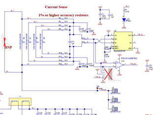
This reference design includes bi-directional dcdc converter. I focused on current sense circuit in below.
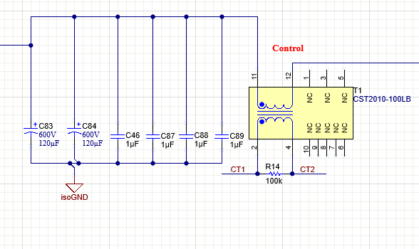
1) I think whole circuit for DCDC side is as below and Ipri is connected to ADC pin in order to control DC link current for peak current mode. I think CT_N and CT_P is floating in normal operation. Could you please confirm?
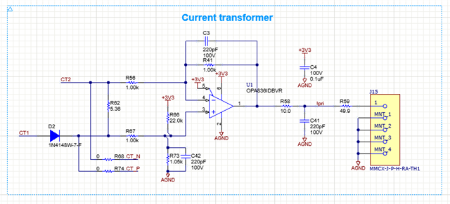
2) How does this circuit achieve positive signal during reverse mode of operation. I think the output of OPAMP will be zero.
3) What is purpose of using R66? How do you decide R66 as 22kohm?
4) Why did you choose R73 as 1.05k and not 1k? How do you decide R73 as 1.05kohm?
Thank you in advance.